• Please review our updated Terms and Rules here

Need advice on how to best clean/de-rust an IBM 5051 w/o damaging it any further

....As best as I could determine, the only +12V tantalum capacitor on the 5150's board is the one next to the mounting hole in the corner between the power connectors and keyboard/cassette connectors.......

On the 64 - 256 5150 board there is 1 tant on the +12V and 1 on the -12V see Modem7's excellent site for a Pic of the 2 tants, Also download the Revised edition April 1984 Technical reference for the 5150 from the same site here. There is a shed load of info on the 5150 and others, Also a superb trouble shooting section.
 
Shunted = in parallel with.

Bypass = shunt to ground. There are two reasons to put a capacitor on a supply rail. The first is decoupling--that is, to decouple the (slow) effects of switching on the power supply, so that they don't interfere with switching., The second is bypassing - getting rid of high frequency signals that are riding the supply rail.

Ah. Thank you! So then I take if from your above comment…

Tantalum caps are still electrolytic, but are better at bypassing high-frequency RF. You could probably replace most of them with plain old aluminum electrolytics shunted by a 0.1 uF ceramic and get pretty much the same effect.

…that ceramic caps are particularly good at bypassing hi-freq RF, which is why the combination of an elco plus a ceramic cap in parallel would work as you described? (If that's right, then I think I've got it now.)

Does anyone still want to elaborate on what exactly those "parasitic effects" of elcos are?
 
I would expect that the schematic is intending to imply that those caps are placed one each adjacent to each bus connector, rather than next to each other.

My "B" board has two (three pin) unused cap locations (marked "CX") one each between every two bus connectors. Only one cap is installed.

I count seven unpopulated three-pin "CX" locations on my board. Maybe it's something like that.

I'm guessing that, once tested, they found the additional caps were not required for noise suppression and the staff in the design department were so excited about releasing the world's first IBM PC they simply forgot to notify the staff in publications about this trivial detail.

That's a good theory. I've also noticed that the prototype board contained a lot of caps; many on the back side too. Maybe we're actually looking at the logic diagrams of the prototype board, which they never bothered to update.

But, as noted before, you can test the basic functionality with no cap in place. An since we are all on the edge of our seats wondering if your board is going to work, I would hope you do this soon!

I've done the testing over the weekend (the news isn't good, but I'm not giving up entirely); I just haven't gotten around to writing that comment yet. I'll try to get to it.
 
Hmm, according to the spec sheet the 75477 driver can sink 500mA so you could use either version, which draw 30mA and 100 mA respectively. The only downside to the H1 is that it's fractionally slower, which doesn't matter in this application. Personally, I'd get the H1 version if it's no more trouble or significant cost, but both will work.
You could measure the coil resistance of the old part with an ohm meter and determine which part is a better match to those resistance values on the spec sheet.

I've done that; I measured 46Ω – like the plain vanilla G5V-2, but unlike the -H1 version. I might try getting the former – if that's even still relevant. See my forthcoming comment (soon to be posted below).
 
…that ceramic caps are particularly good at bypassing hi-freq RF, which is why the combination of an elco plus a ceramic cap in parallel would work as you described? (If that's right, then I think I've got it now.)

Exactly. Generally speaking, design guidelines for TTL call for one 0.1 uF ceramic for every or every other package (you can, or used to be able to, buy sockets with the capacitor included between pins 7/14 or 8/16). Then a electrolytic for every X packages to handle low-frequency issues (X being a value chosen by the designer). The point is that there's no such thing as too much decoupling.

Here's a brief app note that explains things

Also, you should have this easy-to-understand reference: Don Lancaster's TTL Cookbook.
 
Okay, so to finally wrap up what I did over the weekend:

I pulled that +12V cap. Why are they three-legged? It's just that bit harder to keep three solder spots hot at the same time; especially with a primitive soldering iron. Then I retested, but no joy. I actually (temporarily) replaced the +12V cap with that elco I showed earlier (above). Still no joy; no beeps from the speaker.

I then tested the voltages of the P8/P9 plugs while plugged in and powered on. They weren't proper across the board. Was the PSU bad despite the running fan? I didn't think so, because I'd earlier tested the PSU with just a floppy molex plugged into a drive (as a load) – the voltages had been normal everywhere then. So I unplugged the P8 plug from its P1 socket and tested power-up with just the P9 plug in its P2 socket. That caused the voltages to return to normal. I then returned to the excellent -0° MDC guide that was also pointed out by Malc above (thank you), and I noted the P8 voltages: "Power good" pin: .01V; (next pin is omitted/key); +12V pin: .1V; -12V pin: 0V (and the other two are GND). Since the -12V pin read zero, I suspected something afoot there.
An aside: On my PSU, the colours differ from the ones depicted on -0°: I have power good as purple, key omitted, +12V green, -12V yellow, and -5V blue; GND and +5V are the same: black and red, respectively. Maybe that info is a worthy addition to -0°? Modem7?
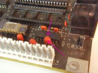
I now took a closer look at the -12V trace's cap. It hadn't blown up, but if you looked closely, you could kind of see what seemed to be a little bulge, plus a subtle minor dark spot:

attachment.php
attachment.php


So since I already knew that the -12V trace seemed to just lead to the extension card slot (position B7, as per above and per TechRef D-21), and since that contact has no trace on my potentially sacrificial CGA-compatible card, I decided to just pull that -12V too and retest.
Removing the -12V tantalum cap turned out to be more difficult than pulling a ****ing tooth, and I ripped out one of the leads, but I got everything out in the end. When I retested, the voltages had returned to normal.

But alas! Still no noise from the speaker, not even when I soldered and wired up another speaker, just in case of a defect of the existing one. (Does polarity really matter with speakers? Because I'm not sure the polarity is correct here.) Also, no picture when I tried a test with the CGA-compatible an the 5153, though the monitor did darken from the blank white OFF state to a blank grey screen on 5150 switch-on.

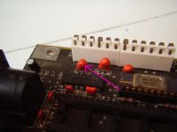
To be thorough, I determined what all the bigger caps were wired to (pre-cap removal and pre-relay cleanup picture). Two of the +5V caps look different. They also have little K's on them. Does that have any significance? (Prolly not.)

Despite the fact that the voltages are all nominal, could the +5V caps still be at fault?
Could the relay still be at fault?
I also had the 8087 present DIP switch wrong for an attempt (because of inconsistent documentation) – could this have caused some lasting damage?
Is there a chance that washing the board as recommended earlier would actually improve its state electronics-wise?

I'm actually thinking now that maybe it was entirely wrong to blame the relay; maybe it just looked bad, but wasn't really. Maybe it was those two 12V tantalum caps – plus some other faults yet to be determined.

I took it from the -0° MDC guide that the heat now should be on the DRAMs, and specifically on the DRAMs in bank 0. What's rather problematic though is that:
  1. I don't actually have any compatible DRAMs to replace those 8KB DRAMs with permanently (some old DRAMs I've still got are incompatible 256KB ones [I take it it's impossible to use those as piggibackers or replacements in any way?], and even the many DRAMs I've got on an AST RAMpage! RAM-card are [presumably incompatible?] 32KB ones) , and
  2. even temporarily using some of the DRAMs from e.g. bank 3 on the 5150 mainboard itself for piggyback-testing of its bank 0 might be a problem, because -0° tells me there are BIOS bugs that actually make the 5150 want all its banks to be fully populated (though DRAM sizes can still vary for varying amounts of RAM). Another problem is that
  3. I don't have an EPROM writer, so do use the SuperSoft/Landmark diagnostic ROM troubleshooting method the MDC guide recommends, I'd have to buy one first – or buy the actual SuperSoft ROM off someone.

It was at this point that I gave in and ordered a relatively (but still reasonably) expensive replacement board off eBay. Clearly troubleshooting and replacing faulty DRAMs is going to be difficult, and I don't even know for a fact that that's now the problem, or the only problem, and once I've ordered a ROM and DRAMs (that I also have to find first), I'll have spent a lot of time and some money, and there's a real danger that I'll run out of steam before I get that 5150 running again, so since I'm already ordering various components, let's make hay while the sun is shining, grit my teeth, bite the bullet and swallow the "bitter bill" [sic]. ;-)

However, though this spending splurge will hopefully get my 5150 restoration back on track, my ordering that replacement board does not mean that I've entirely given up on the old one yet – because it also occurs to me that between a bunch of components I got (e.g. a spare PSU and keyboard from a 5155, etc.), with that board, I'm a monitor shy of a second PC. That second PC would be a bit of a Frankenputer; not in its original case, and with odd clone cards, etc, but still. The prospect is enough reason not to give up on Þe olde maine boarde just yet.

If I read that -0° page on those BIOS bugs correctly, bug 1 shouldn't prevent me from booting to BASIC at least, correct?

Also, does what it says under "Symptoms" for bug 2 mean that I could maybe remove all the DRAMs from bank 3, set SW1 and SW2 for one bank only, and maybe also not see that 201 error? Is that error a halting one – i.e. will it prevent me from booting to BASIC at least? Given encouraging answers to that one, I'll probably try piggy-backing around and see if I can get something more than no beeps and no picture.

If that doesn't work, then in time, I may order that SuperSoft ROM off someone, but that's probably not going to be soon. I hope to get the non-Frankenputer 5150 up and running with the replacement board before then, and I hope I'll be able to report back how I'm getting on, and then return to case cleaning and restoration as well.

Then you very much for your help, everybody, and if you can still help even more by answering any of the above questions, please do! :)
 

Attachments

  • P7090001.jpg
    P7090001.jpg
    93.2 KB · Views: 1
  • P7090003.jpg
    P7090003.jpg
    83.8 KB · Views: 1
Last edited:
I pulled that +12V cap. Why are they three-legged?
The principle behind the three legs is explained at [here] - an improvement in high frequency performance. However, per that web page, in order to get that improvement, the capacitors need to be used by the board engineers in a certain way, and maybe IBM has not done that.

It's just that bit harder to keep three solder spots hot at the same time; especially with a primitive soldering iron.
I think that most people use a pair of side cutters to clip the capacitor body off, leaving three legs sticking out of the board, legs that can then be removed individually.

Maybe that info is a worthy addition to -0°? Modem7?
I will 'take it on board'.

Does polarity really matter with speakers?
It does for a multi channel audio system, but not for a computer motherboard.

Despite the fact that the voltages are all nominal, could the +5V caps still be at fault?
The ones near the RAM chips are very important. If one of those has failed open circuit, then the base 16K RAM test done by the POST could be failing.
If it is failing, you would see a 'motherboard appears dead' symptom.
But then, the failure of any one of many components on the motherboard can produce the same symptom.

Could the relay still be at fault?
No.

I also had the 8087 present DIP switch wrong for an attempt (because of inconsistent documentation) – could this have caused some lasting damage?
No.

If I read that -0° page on those BIOS bugs correctly, bug 1 shouldn't prevent me from booting to BASIC at least, correct?
Correct. Neither bug will produce a 'motherboard appears dead' symptom.


The voltages are correct, and presumably that includes the POWER GOOD line. So, what normally happens is:
1. The rising POWER GOOD line takes the motherboard out of the RESET state.
2. The 8088 jumps to a particular address, which is in the BIOS ROM.
3. The POST in the BIOS ROM starts to execute.
4. The POST progresses as shown at [here].

Maybe your motherboard isn't even getting as far as step 2. Maybe the POST is starting but failing one of the early tests.

This is the point where I would be using the SuperSoft/Landmark diagnostic ROM. If that ROM does not display anything (or at least beep), then there is something very seriously wrong with the motherboard. If the ROM does display something (or beeps), then there is a way forward (but no guarantees of a fix though).
 
......An aside: On my PSU, the colours differ from the ones depicted on -0°:....I have power good as purple, key omitted, +12V green, -12V yellow, and -5V blue[/URL]; GND and +5V are the same: black and red, respectively.....

Looking back at post #10, The pic of the PSU you posted looks like a 130W PSU as fitted in the IBM XT 5160, possibly a "SCHRACK" ?, Back in the day it was a common upgrade to replace the original 63W 5150 psu with the 130W psu for people wanting the more power hungry Hard drives fitted to their 5150. Hence the difference in colours between your psu and the clone compatible that Modem7 used in the guide. Actually my original 63W 5150 psu has exactly the same colour wires as in the pic in Modem7's guide except of course mine has the empty key slot, But that's not really important considering the masses of clone / compatible psu's available and not all manufactures used the same colour code.The most important thing is the output voltages of your psu must be within spec with the psu loaded.
 
Back
Top