• Please review our updated Terms and Rules here

PDP-11/35 - The real fun has begun

Twylo

Experienced Member
Joined
Feb 12, 2009
Messages
230
Location
Poulsbo, WA
Hey folks,

Well, I've been real busy on my PDP-11/35 for the last couple of months. I basically had to take the whole thing apart, down to the very last screw, clean everything, get the chassis sandblasted and powder coated, repair the power supply, and put it all back together. It was a lot of work, but it was worth it. And Tonight was The Big Night -- it was the first time that I powered it on with the CPU board set installed.

It did not work. Not that I expected it to, and yet I'm still somewhat disappointed, I guess.

Now, when I say "it did not work", what I mean is that it powered on, and nothing exploded. Random lights on the front panel latched on. The "Run" light was on, which was clearly a lie because it was not running. The only input that has any effect at all is the "Start" switch - when depressed and held down, all the LEDs dim just a little bit, and when it is released, a new seemingly random state appears on the front panel lights. That's something, I guess! No other front panel switches do anything.

Now, my first question for the group is, what is the absolute minimum possible configuration to debug the CPU in? Is it possible to bring up the CPU with no memory installed, just for testing?

For example, here's the configuration I tried:

System Backplane (9 Slots):

  1. Empty
  2. Empty
  3. M7232 Micro Word Module
  4. M7231 Data Paths Module
  5. M7233 IR Decode Moduel
  6. M7235 Processor Status Module
  7. M7234 Timing Module
  8. Empty
  9. [A-B] M9302 Terminator, [C-F] M7800 Async Serial

(For comparison, the original configuration as I received it is documented here: http://www.loomcom.com/blog/2012/04/30/pdp-1135-details/)

Is a Grant Continuity card required in 8D? I didn't think it was, but...

Even so, would a failure of grant continuity cause the symptoms I'm seeing? I really didn't think so.

Anyway, once I confirm whether this configuration is a valid test, I will move on and try to find a board extender so I can start digging into the logic a little.

This is intimidating!

-Twylo
 
On the Console Switch Register:


  1. Flip the HALT switch down.
  2. Depress the START and release

Please answer:


  • What do the lights show?
  • Did they change behavior?

More:


  • Set a Pattern in 0-17
  • Toggle LOAD ADDR and release

Do lights follow pattern?
 
Last edited:
On the Console Switch Register: [...]

Hi RSX11M+!

I hope this answers your questions. I just ran downstairs and took this video (the 11/35 is propped up on its side for easy backplane access at the moment)


Short answer:

1. Each depress/release of the "START" seems to jump between a set of states (possibly floating inputs somewhere), the states do not seem to be consistent between power-ups.

2. LOAD ADDR seems to do nothing.
 
Ok, slightly functional. Doesn't seem to be processing Address. I'd start there.

Insomniacs rule! [which is why I'm going to sleep] I'll look over some manuals tomorrow. Maybe I'll have some better suggestions.

Got any memory for that system?
 
Insomniacs rule! [which is why I'm going to sleep]

Yes we do! Well, actually I'm going to bed myself as soon as I close this browser window (that's what I said an hour ago...)

Got any memory for that system?

I do, yes, 32KW of MOS memory. If I plug that in I'll need to get some more grant continuity cards so I can fill out the empty backplane slots in the last backplane (a DD-11A). (Actually, I guess I can always just use jumpers on the wire-wrap side temporarily if I need to, until I can get some more G727A's)

Many thanks for the replies! It makes me feel better that someone else is thinking about this too :)

-Twylo
 
I’m certainly amazed at how quickly you’re moving on this project. It looks like you have a substantial part already finished and working.

You are correct in that an absolute minimum configuration should not require memory. It should also not require any grants, terminator or serial line unit.

Here’s something though that you may find interesting. An 11/40 is unique in that the run light does not indicate when the processor is executing instructions but rather when the process clock is running (which is pretty much all the time unless it is waiting on the bus) and this includes when it is looping in the console routine. So if you were in front of a functional box that was physically halted, you should expect to see RUN (clock running), PROC (processor in control of the bus), BUS (bus in use) and CONSOLE (processor executing in console mode) all illuminated. (I realize you don’t see that now of course.)

So, is there any possibility that this particular machine ever had memory management (M7236) installed? It probably is a long shot, but installing the MMU requires a number of jumpers on the other modules to be changed. If those jumpers are set for MMU but MMU is not physically present, the console behaves very strangely. (Ask me how I know this.)
 
You are correct in that an absolute minimum configuration should not require memory. It should also not require any grants, terminator or serial line unit.

No terminator? Is that because the KD11-A backplane isn't attached to any Unibus, so there's no Unibus to terminate? Hmm, interesting!

Here’s something though that you may find interesting. An 11/40 is unique in that the run light does not indicate when the processor is executing instructions but rather when the process clock is running (which is pretty much all the time unless it is waiting on the bus) and this includes when it is looping in the console routine. So if you were in front of a functional box that was physically halted, you should expect to see RUN (clock running), PROC (processor in control of the bus), BUS (bus in use) and CONSOLE (processor executing in console mode) all illuminated. (I realize you don’t see that now of course.)

Wow, that's fascinating... I should have read the manual more closely regarding the run light, then.

So, is there any possibility that this particular machine ever had memory management (M7236) installed? It probably is a long shot, but installing the MMU requires a number of jumpers on the other modules to be changed. If those jumpers are set for MMU but MMU is not physically present, the console behaves very strangely. (Ask me how I know this.)

That's a really good question. It certainly didn't have any when I received it. My guess is that it did not, because it only came with 32KW, and only one memory backplane was installed. But I will inspect the backplane and look for the jumpers just in case. Thanks for the tip!

-Twylo
 
Sounds like KM11 is more dead familiar with the 11/35/40 than I, although I can confirm his description of the RUN light [only indicated presence of Clock on this model], and his thinking of checking jumper settings of the existing cards / slots for lack of MMU, FP and EIS, etc.

I was not as sure about the CPU registers operating correctly without memory. I will defer to his experience on this.
 
I can now confirm that there was never a KT11-D, KE11-E, or KE11-F option installed. I checked for all the changes that would be required when installing these options, and they're not there. So we can rule that out, at least.

-Twylo
 
Looking at schematics... please re-verify cables on KY11-D Console J1 to J1 of M7231, and J2 to J1 of M7235 for condition, unbroken pins, seating, and correct orientation.

Would you feel comfortable following the LOAD ADDR signal from J2-AA on the KY11-D through to the M7235 board with a scope or meter?

You don't by chance have a HEX Extender board set, do you? [perhaps I should be following your progress on your links]

Just trying to get some ideas.
 
Looking at schematics... please re-verify cables on KY11-D Console J1 to J1 of M7231, and J2 to J1 of M7235 for condition, unbroken pins, seating, and correct orientation.

Before re-installing them, I checked continuity on all lines of the cables between the KY11-D and the M7231/M7235, because I was worried about just such a problem. I'm 99.9% sure I have the orientation correct based on my original photos, and on the schematics (essentially the two ends are rotated 180 degrees - Pin A on KY11-D J1 goes to Pin VV on M7231 J1, etc.), but I'll double-check again anyway. Another physical inspection can't hurt!

Would you feel comfortable following the LOAD ADDR signal from J2-AA on the KY11-D through to the M7235 board with a scope or meter?

You don't by chance have a HEX Extender board set, do you? [perhaps I should be following your progress on your links]

Just trying to get some ideas.

Sounds like a good idea, and I'd be comfortable doing that. Unfortunately I'm stuck at the moment because I don't have a hex extender board set. Someone is going to lend me one, but it probably won't be here until next week. I'd like to get debugging sooner, but patience is a virtue. Or so they tell me :)

-Twylo
 
It seems like you ruled out the jumper configurations and are currently on a mission, so I don’t want to distract you. Just as a follow-up to your terminator question though, the UNIBUS can be characterized as a transmission line (multiple lines actually) and “a uniform transmission line terminated in its characteristic impedance will propagate an electrical signal without reflections”. Accordingly, Digital’s spec stated that the UNIBUS must be terminated at both ends. In your example of “absolute minimum configuration”, you still have a UNIBUS but the processor (which also provides termination) constitutes both the start and end of the bus – a trivial case. In reality, a short lightly loaded UNIBUS will generally operate just fine when only terminated at one end. This is useful to keep in mind when testing but I would not advocate leaving it that way. At this point in your troubleshooting however, I think I would remove everything that is not essential.
 
It seems like you ruled out the jumper configurations and are currently on a mission, so I don’t want to distract you. Just as a follow-up to your terminator question though, the UNIBUS can be characterized as a transmission line (multiple lines actually) and “a uniform transmission line terminated in its characteristic impedance will propagate an electrical signal without reflections”. Accordingly, Digital’s spec stated that the UNIBUS must be terminated at both ends. In your example of “absolute minimum configuration”, you still have a UNIBUS but the processor (which also provides termination) constitutes both the start and end of the bus – a trivial case. In reality, a short lightly loaded UNIBUS will generally operate just fine when only terminated at one end. This is useful to keep in mind when testing but I would not advocate leaving it that way. At this point in your troubleshooting however, I think I would remove everything that is not essential.

I have not ruled out jumper issues. We checked the ones that you suggested, and that I too saw from my quick scan of the documentation. Believe me, I wish I had more of your first hand knowledge of this machine to help. Please feel free to redirect our efforts.


Before re-installing them, I checked continuity on all lines of the cables between the KY11-D and the M7231/M7235, because I was worried about just such a problem. I'm 99.9% sure I have the orientation correct based on my original photos, and on the schematics (essentially the two ends are rotated 180 degrees - Pin A on KY11-D J1 goes to Pin VV on M7231 J1, etc.), but I'll double-check again anyway. Another physical inspection can't hurt!

These BERG connector conventions are a constant source of concern on vintage DEC equipment. I believe it is essential to verify this [and other] signals by proving they appear where they should on the boards at both ends of the cable.

A mistake I often see is to presume equipment was correctly configured on receipt. Unless you have some assurance that it was operational as configured, you could have a "Frankenputer" on your hands. It makes me giggle to think of the poor engineer who ended up with some of our dis-used equipment. Stuff we made work together that had no business occupying the same chassis, would have been confusing enough, let alone "bulkheadized" connector schemes that looked so original they might be mistaken for such.

Be very suspicious - it helps.

Sounds like a good idea, and I'd be comfortable doing that. Unfortunately I'm stuck at the moment because I don't have a hex extender board set. Someone is going to lend me one, but it probably won't be here until next week. I'd like to get debugging sooner, but patience is a virtue. Or so they tell me :smile:

-Twylo

A way to proceed before you receive the extenders would be to pull the boards from the chassis, but still connected via the cables and use a VOM to check signal paths exist as they should. It can be a little tricky, because you're trying to distinguish between the low impedance the cable presents with the low impedance un-powered circuitry does. I usually find a digital VOM that can resolve tenths of an ohm, or has a special "low current" ohm scale will do nicely at this. Another trick is to reverse polarity - A "cable based" path won't change readings when this is done, where a sneak path through chips to power supply impedance will.


Incidentally Twylo, these BUS extenders can still be purchased and since you seem to be in this "for real" you should consider owning a set. Buy one QUAD and one DUAL and they'll be useful for QBUS too.
 
I just bit the bullet and ordered dual width and quad width extender cards from Douglas Electronics. They should be here on Friday or maybe Monday. That plus the hex extender that's being lent to me next week should be plenty good enough for all my debugging needs!

-Twylo
 
I appreciate your kind remarks RSX11M+, but if you’re keeping track you’ll notice that I haven’t exactly provided a silver bullet to anyone on this forum yet. As such, it’s not my intention to derail a moving train here, but there are a few things that bother me. If we are to believe the lights shown in Twylo’s little video (and that’s admittedly a huge leap of faith), the console never really gains control, so I wouldn’t expect LOAD ADRS, EXAM or DEP to (visibly at least) do anything. To me, the bigger question is why nothing changes when ENABLE/HALT is moved to the HALT position. It appears that subsequently pressing START does attempt to initialize the bus (I see PROC and BUS go on) and that certainly seems like a good sign. So if I were to start tracing anywhere, my tendency would be to focus in the ENABLE/HALT area first.

BTW, where to you guys work anyway? I see posts from all hours of the day and night! :)
 
Not speaking for others - I don't work. [not exactly happy about it - but it's the world we live in]

I agree totally about your analysis of the video. My thinking is to find out why the panel doesn't respond as it should. First step is to verify that the cables are installed correctly. Although one cannot count on it, DEC usually tried to design pinouts that wouldn't be damaging if reversed or transposed. Of course, I've seen a lot of melt-downs too, people can be more creative than engineers give them credit for.

Anyway, when he's ready this issue can be resolved. Hopefully, replacement parts won't be involved.
 
Please bear with me on this lengthy [and somewhat redundant] post. It's necessary because of the potential consequences.

...I'm 99.9% sure I have the orientation correct based on my original photos, and on the schematics (essentially the two ends are rotated 180 degrees - Pin A on KY11-D J1 goes to Pin VV on M7231 J1, etc.)...

I was going to post immediately when I saw this, but decided that since it was already powered like this, to wait until I'd taken additional steps.

I've spoken to a friend who I worked with on UNIBUS PDP-11s, and we discussed this at some length. His sense, and mine, is that from the symptom and our shared knowledge of DEC cabling inconsistencies, that there is a high likelihood that one or both of these cables is incorrectly inserted.

We discussed situations we'd found in our own DEC equipment where cables had been manufactured with the connector ends swapped. (Connectors in PC boards too) This is difficult for those in a "post-BERG" world, where AMPHENOL standards are prevalent, to appreciate. Such cables were sometimes manufactured with no visible "BAR" on the actual cable, making judgment of correct installation highly subjective.

So it comes down to this... It would be reckless for me to advise you to "Flip" a cable" based on my speculation, as damage could result if I'm wrong, but at the same time we need to resolve this question because if it is wrong - it's the solution, at least in part.

Hence my previous recommendation to test the result by VOM in an un-powered mode. Basically, you need to somehow assure that signals end up on the correct board components, after passing through these cables.

Detailed photos of the boards, with connector markings legible and of the assembly with cables in place would be helpful in allowing me (us) to be more involved in helping. Even so, the VOM is the most conclusive, and harmless, test method.
 
I've spoken to a friend who I worked with on UNIBUS PDP-11s, and we discussed this at some length. His sense, and mine, is that from the symptom and our shared knowledge of DEC cabling inconsistencies, that there is a high likelihood that one or both of these cables is incorrectly inserted.

We discussed situations we'd found in our own DEC equipment where cables had been manufactured with the connector ends swapped. (Connectors in PC boards too) This is difficult for those in a "post-BERG" world, where AMPHENOL standards are prevalent, to appreciate. Such cables were sometimes manufactured with no visible "BAR" on the actual cable, making judgment of correct installation highly subjective.

OK, I’m on board with you here – let’s see if we can put this cabling question to rest. If those cables are OEM, then each should be a BC08R which is a 40-conductor ribbon cable with a shield on one side. The side with the shield is easily identified as being smooth in contrast to the opposite side which is ribbed. Socket A of the connector is always on your left as you hold the cable smooth side facing you with the connector of interest at the top - socket VV is on the right. This is true regardless of which end you look at. So assuming that the cables are currently assembled the way DEC originally specified, the correct orientation at all termination points (console and processor modules) would appear to be with the ribbed side closest to the board and the shield facing outward.
 
We can cross reversed cabling off the list. I took some time this evening to perform continuity tests between the KY11D and the M7235 and M7231, and I'm 100% certain the cables are in the correct orientation.

Evidence:

  1. The KY11, M7235, and M7231 are all clearly marked "SHIELD TOWARD BOARD" next to their respective BERG connectors. The cables are real DEC shielded BC08-R cables, and made sure that the shield was toward the board in all cases.
  2. I measured continuity from pin 6 of E2 (7410) on the KY11 to pin 11 of E6 (7474) on the M7235 (this is the START switch)
  3. I measured continuity from pin 6 of E5 (7410) on the KY11 to pin 11 of E9 (7430) on the M7235 (this is the EXAMINE switch)
  4. I measured continuity from R50 on the KY11 to pin 3 of E26 (DEC 380) on the M7231 (this is bit 8 of the DATA LEDs)
  5. I measured continuity from R34 on the KY11 to pin 2 of E93 (DEC 380) on the M7231 (this is bit 0 of the DATA LEDs)

These measurements were made with power off using my Fluke 79III on the continuity testing setting, and all measured < 0.1 ohm. So I'm convinced cabling is right.

If my board extenders get here tomorrow (as I hope they do!) I will start tracing signals with the power on. I should be able to follow the output from the ENABLE/HALT switch and the LOAD ADRS switch and see where they disappear into the aether.

-Twylo
 
Last edited:
This may also be a source of some confusion...

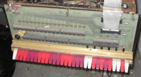
I have been saying that I have the KY11-D console. This is incorrect, I don't! I have the KY11-K console. My console has the BERG connectors on the right, and the power connector on the left. I've attached a photo of the original not-cleaned, horrifyingly dirty state. (It looks MUCH BETTER now :^) )

ky11k.jpg
 
Back
Top