• Please review our updated Terms and Rules here

PDP-8 core memory troubleshooting

More interestingly the "Adder Test" maindec-8e-d0ca-pb also outputs readable text:
I'd probably have used d0cc, as it's a little newer. Don't think that's your problem, though.
Unfortunately after about 30 minutes it then halts in what I think is (or should be) the "False Carry Test" (FCT).
Strangely the halting address 3306 is not shown in the listing in maindec-8e-d0ca-d.pdf which has a gap between 3270 - 3400.
It is halting right in that gap in the listing.
A quick check of the memory map on page 61/66 confirms that the diagnostic does not load into location 3306. Running the 'mmap' tool on the actual binary file agrees with the PDF.

This means that the document and the BIN file don't match up or that the Lab-8/E has a very weird fault. Note that it passes the first two tests.
It looks to me like the latter, less desirable situation.

Vince
 
It may be wise, if possible, to confirm that you're loading the same file I've got. Perhaps you could run mmap from http://svn.so-much-stuff.com/svn/trunk/pdp8/8tools/ on your binary and seeing if it matches the map near the end of the PDF?

Vince

Thanks Vince,

I tried your mmap tool and it shows the two regions (PC = 3306 and AC = 2740) as unoccupied.
Of course the maindec-8e-d0ca-pb diagnostic could use these "gaps" to dynamically generate a set of instructions and then jump into those locations.

I have built the PDP-8 version of SIMH under Windows, but haven't yet figured out how to load and run the diagnostics into SIMH.

I have an SBC6120 I could try, but have no serial cable for it. I will have to figure out the serial cable pin-out.

Thanks to all of you who helped me along my steep learning curve.

Best regards
Tom Hunter
 
I have built the PDP-8 version of SIMH under Windows, but haven't yet figured out how to load and run the diagnostics into SIMH.

You should find that the BIN format image file name works as a target of the SIMH "load" command.
From there, it's not hard to get it running.

Vince
 
You should find that the BIN format image file name works as a target of the SIMH "load" command.
From there, it's not hard to get it running.

Vince

Hmmm - the maindec-8e-d0ca-pb diagnostics works fine in SIMH, so this means that the Lab-8/E has some rather odd and subtle fault and wanders off into unchartered territory. :-(
I will try Doug's suggestion and test memory to make sure it is perfect before running any other tests.

Actually now I wonder if my board setup is to blame. At this moment it is very warm here in Perth in Western Australia.
My electronics workshop is at about 28 degrees C but this quickly goes up to over 30 degrees when I run the Lab-8/E.
To avoid any overheating I have moved the boards so that they are right beside the two power supply fans (except for the front-panel and M8655 boards which I placed in the back).

So the board order is:
First Omnisbus: front panel, 14 empty slots, M8330, M8310, M8300, M837, M849
Second Omnibus: 2 empty slots G11C, H212, G233E (core memory), 5 more empty slots and the M8655, 3 more empty slots and the M8320.

Now the manual clearly states that the CPU boards meant to be in the front next to the front-panel board.
I wonder if this is critical and could cause the type of problem I am seeing.

Thanks and best regards
Tom Hunter
 
I would not be too clever...

Set the cards up as per the manufacturer’s recommendations (slots etc).

Follow Doug’s advice and configure the minimal system to start with.

The problem you have is that you need operational CORE to run the CPU diagnostics and an operational CPU to run the CORE diagnostics. Trying to run the CPU diagnostics with faulty CORE may give strange and inconsistent results (as Vince and Doug have already pointed out).

If things are overheating, you need to add a fan to cool things down...

You can either run the CORE memory test (this may still give inconsistent results though) or (as I would initially recommend) the earlier initial CPU instruction tests (that did appear to work) for a longer time (say 2 hours) to see if they start to fail. If they do, we have a heat-related issue to track down.

Dave
 
So the board order is:
First Omnisbus: front panel, 14 empty slots, M8330, M8310, M8300, M837, M849
Second Omnibus: 2 empty slots G11C, H212, G233E (core memory), 5 more empty slots and the M8655, 3 more empty slots and the M8320.

You don't need the M837 until you start testing beyond 4k. Everything else is necessary.

I don't think the card placement you have chosen should be a problem. But if everything is working properly the cards are not all that sensitive to heat. If the temp is ok for you to sit next to the machine then the machine should be ok. If you can't stand to be in there then it is probably too hot. With that in mind I would put the cards back in their recommended positions.

You didn't mention if you have placed a cover on the machine. The airflow without a cover is not really through the cards and the side away from the power supply is not cooled as well. A cover will help force the air to flow between the cards. This is not usually an issue but if you have a marginal component every little thing can cause an issue. Simply placing a sheet of cardboard on top will greatly increase airflow over the boards. But all this will do is help verify the issue is heat related.

If the issue is heat related then you have the next issue of those darn top connector blocks making it difficult to place a single card on an extender. An alternative is to spot cool components using freeze spray. They used to sell Freon in an aerosol spray can with a long tube for this purpose. If you can find a simple test case that fails then this is a really quick way to localize to a single part. Alternatively you can use a heat gun with a small nozzle to spot heat parts. It is surprising how quickly this can work. In your case you run your test and then start spot heating components. Instead of a half an hour you get a result in a few seconds. Just don't overdo it. Heat is the enemy of old IC's.

I mentioned previously that it often helps to zip memory to halt instructions before you load diagnostics. That way you get an instant halt if it goes off into the weeds. If the word before the hlt address is not a halt then the problem was probably an issue with JMS. This helps stop further corruption of memory.
Code:
    1        7600          *7600
    2 07600  1204  LP,     TAD HALT
    3 07601  3606          DCA I ADDR
    4 07602  2206          ISZ ADDR
    5 07603  5200          JMP LP
    6 07604  7402  HALT,   HLT
    7 07605  0000  ADDR,   0
    8                     $
That will set memory from 0 to 7600 to a halt instruction. Don't run it a second time without resetting 7600 and 7605. This is the shortest sequence I could come up with. It ends by overwriting the TAD HALT at 7600 with a hlt so the next time the JMP LP is executed it halts.

If you get a hlt that is not part of the diagnostic then the program didn't run correctly and the chances are high that you have a memory problem. Either it did not read correctly or the writeback was corrupted and things went south the next time that memory location was read. It can sometimes help to take a memory snapshot after you load but before you run the diagnostic and then another after the crash. Run a diff on the two images to see what has changed.
 
My problem is caused by a core memory fault. My fixes to the sense/inhibit board fixed the 12 data bits, but there appears to be also a problem on the X/Y driver board (hopefully not on the core board itself).

Addresses 3200 - 3277 read back as all zeroes no matter what I write into those locations. I suspect some address decoding issue on the X/Y board.

Best regards
Tom Hunter
 
So it sounds like a bit of the MAINDEC code is missing then... There’s yer problem...

I think you are on the right track with regards to the address decoding somewhere.

If it is as simple as a range of addresses, then use the front panel deposit key with your scope / logic analyser to checkout the address decoding circuitry.

Dave
 
It looks like my problem with the address range 3200 - 3277 is caused by a faulty core selection diode array on the H212 core board itself.
The diode arrays (E1 - 24) are DEC 2501 (DEC part number 19-10010-00).

I am trying to work out the exact diode array responsible for locations 3200 - 3277 from the MM8-EJ schematics. Any second opinion or confirmation would be appreciated. :)

Does anyone know if these DEC 2501 (or DEC 2501-1) are still available maybe as a non-DEC part?

Alternatively there is also a chance that I have a broken X selection core wire for this address which strings together the associated 768 cores.

I am somewhat intimidated by the H212 board. I was hoping to handle it as little as possible as it is the most sensitive part of the entire system.

Thanks and best regards
Tom Hunter
 
I have figured out the diode address decoding scheme. The responsible diode array is E11.

The good news is that the diodes in E11 measure good.

The bad news is that the core line is open circuit (between JT2 and and pin 9 of E11). All other core wires connected between JT2 and their respective two diodes measure about 5 Ohm.

The really bad news is that I cannot trace the PCB track coming from pin 9 of E11 to any of the core wires. The track disappears underneath the core mat and I cannot see it emerge anywhere. Using a multimeter I checked all the core connection points trying to find where pin 9 of E11 connects to but no luck. This may actually mean that the PCB track is itself open circuit, but without knowing to which core wire it is meant to be connected I cannot patch it.

I will try to locate the core connection point again when I recovered from the current ordeal. It requires a steady hand, magifying goggles and extreme concentration. I really don't want to rip any of the core wires.

Does anyone have a suggestion on how to move forward?

Is there a more detailed document than the "MM8-EJ_Engineering_Drawings_May73.pdf" from Bitsavers?

It would be nice to understand the physical core layout and the wire connection points. A photo of a blank H212 PCB would be a nice alternative (or a PCB with the core mat removed from it to show the tracks on the component side now obscured by the core mat and its white plastic carrier).

Sigh - I did not expect having to dive quite this deep.

Thanks and best regards
Tom Hunter
 
Tom,

Confirmed: 5 Ohm between E11 pin 9 and JT2.

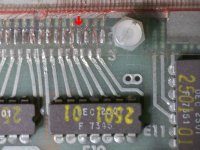
I measured 0 Ohm between E11 pin 9 and the 4th from right inner pad (red arrow in image) above E10 when E10 is towards you with E11 to the right.

202101072122_h212_E11p9.jpg
 
Tom,

Confirmed: 5 Ohm between E11 pin 9 and JT2.

I measured 0 Ohm between E11 pin 9 and the 4th from right inner pad (red arrow in image) above E10 when E10 is towards you with E11 to the right.

View attachment 65629

Thank you Kevin!

I don't know why I missed this when I originally tried to locate the pad.
The other end of the core wire is just opposite the pad you found.
Sadly measuring between those two pads I see an open circuit.
All other wires coming from E11 measure 5 Ohms as expected.

There is a small chance that there is a cold solder joint on either end of the offending wire, but I won't get my hope up. The solder joints look nice and shiny.

I will disregard the "Warranty void if seal is broken" stickers and attempt to reflow the solder on both ends. I guess it is a few years too late to claim warranty on it. :)

If the reflow attempt doesn't fix it, then I can still use the core memory to play except that I have to be aware of the hole between 3200 and 3277.
Of course MAINDECs which use this area won't run so I cannot fully check-out the rest of the system. Also OS/8 won't be happy with the hole. :-(

Thanks again for your help
Best regards
Tom Hunter
 
I have tried to reflow both sides without any improvement.

I have even attempted to solder a bit further back on the pad by applying liquid flux and cranking up the soldering iron to 400 degrees C to burn off the insulation, but no change.

Visual inspection of the section of core were this X wire goes through does not show any damage.

This is a disppoining finale after having fixed two different problems on the sense/inhibit board now I have an unfixable broken core wire. :-(

Thanks to everyone who helped.

Best regards
Tom Hunter
 
This is a disppoining finale after having fixed two different problems on the sense/inhibit board now I have an unfixable broken core wire. :-(

A quick off-the-cuff thought for a low cost solution. I have not researched the practicalities; but if I owned the machine and it was in this situation then this is one option I would definitely explore before giving up!

Modify the address handling logic at the OMNIBUS side so that the bad patch is in the upper 4K. I don’t think it would be able to tell that this has been done? I suppose it might be possible to make the (now bad) upper 4K "disappear".​

If that works out, at least it could end up as a properly working system, even if it currently only had 4K of memory.

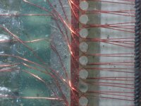
I wonder what has happened to that one wire? If you cannot see any damage in the "mat" or along the wire, maybe the problem is at the posts (in the middle of the following image). Has it snapped there, maybe?
20210108_h212cores2.jpg

Be wary of heating the wires; they are touching each other...
 
Looking at the schematics for the H212 (MM8-EJ) I see that EMA2 appears on drawing sheet 3 and is coupled to E14 pin 9 via wire link W1.

EMA2 should select between the upper and lower 4K banks.

I am just thinking out aloud here...

If W1 is removed - could we strap E14 pin 9 to ground or a convenient VCC pull-up resistor to make it a HIGH 4K or LOW 4K card - with the operational 4K appearing in the low addresses?

This might overcome the initial problems whilst we work on a full rectification for the other 4K half. Reversal should then be simple enough?

You really need to fix the problem in some way or another - otherwise you will be stuck running your own programs (as real-world programs - e.g. the assembler and compilers) will use this memory area and crash.

EDIT: Doesn't E11/9 connect to E10/3 and E10/4 connect to E11/10? This then goes off to the core stack on XPRD3? With E10 being an IC transformer and E11 being a transistor array? Or am I on the wrong schematic?

Dave
 
Last edited:
Just as a different comment. I do know that I've read about people repairing the actual core mat as well. So it's possible, even if not the must fun thing.
 
A quick off-the-cuff thought for a low cost solution. I have not researched the practicalities; but if I owned the machine and it was in this situation then this is one option I would definitely explore before giving up!
Modify the address handling logic at the OMNIBUS side so that the bad patch is in the upper 4K. I don’t think it would be able to tell that this has been done? I suppose it might be possible to make the (now bad) upper 4K "disappear".​

If that works out, at least it could end up as a properly working system, even if it currently only had 4K of memory.

I wonder what has happened to that one wire? If you cannot see any damage in the "mat" or along the wire, maybe the problem is at the posts (in the middle of the following image). Has it snapped there, maybe?

I very carefully checked along the section of core and the posts for any visible damage using magnifying goggles looking through a magnifying light. I don't quite get the same magnification as your amazing photo (what did you use to make that?), but the broken wire is not obvious. On the JT2 side their are two wires connected for each pad. The wire associated with 3200 - 3277 is open circuit. Its "paired" wire associated with 3300 - 3377 measures 5 Ohm.

I agree that I could relatively easily turn the 8k core into a 4k core but fortunately the owner of the machine found in "box 13" (note the lucky number) of his collection a H212 among other non-PDP-8 boards. I picked up the board and it seems to work at least so far that I have successfully run through:

8E-D0AA "Instruction Test I & II"
8E-D0BA "Instruction Test II"
8E-D0CA "Adder Test"
8E-DLEA "Memory Address Test"

The last two failed on the faulty H212, but ran fine on the "new" board.

Then I run 8E-DLAA "Checkerboard Test" and it immediately failed in an undocumented way in an unused location. From then on nothing worked at all not even the RIM loader.

It is quite warm in my electronics lab so I let the machine cool down, opened my study next to it with the aircon on full blast and use a fan to try to redirect some of the cold air into my lab. I have also setup a small fan blowing directly at the core memory section of the machine. The tests above run fine again and so did the "Checkerboard Test".

I remember reading that the MM8-EJ is a matched kit. I wonder if the "Checkerboard Test" failed because the MM8-EJ kit is now slightly mis-matched with the new H212.

Thanks and best regards
Tom Hunter
 
Back
Top