• Please review our updated Terms and Rules here

PET 2001 keyboard issue + instability

Oswald

Experienced Member
Joined
Mar 18, 2022
Messages
65
Update on the cassette situation: I've been able to get the PET drive to save cassettes fairly reliably (though still with occasional errors/corruption) but haven't once gotten it to load. I've cleaned the heads, fiddled with the capstan roller, changed the belt, and still no luck. Any ideas what I should do next?
 
Last edited:

Oswald

Experienced Member
Joined
Mar 18, 2022
Messages
65
Any chance of posting your 'fix' for others?
Replaced R3 in Matthew D’Asaro's PET video mixer schematic with a 210 ohm resistor, but I later realized the problem was happening because I was injecting 9v instead of 5v... oops!

I also added an LM386, speaker and line out for audio, sounds great!

Now if I can just get this tape drive working...
 

Attachments

  • petvideoadapter.png
    petvideoadapter.png
    18.8 KB · Views: 12
  • IMG_5425.jpg
    IMG_5425.jpg
    1.2 MB · Views: 9
  • IMG_5426.jpg
    IMG_5426.jpg
    1.8 MB · Views: 10
  • IMG_5439.png
    IMG_5439.png
    3.8 MB · Views: 10
Last edited:

Oswald

Experienced Member
Joined
Mar 18, 2022
Messages
65
I ended up removing the resistor entirely and that fixed it. It wasn't present in the original CB2 audio schematics from the 70s, which makes me wonder why it was added.
 

Attachments

  • pet-composite-video-adapter.jpg
    pet-composite-video-adapter.jpg
    17.4 KB · Views: 7

Hugo Holden

Veteran Member
Joined
Dec 23, 2015
Messages
4,158
Location
Australia
I really don't like those designs at all.

Ideally the H and V sync are mixed with an XOR gate or the H sync gets abolished during vertical sync time.

But the other problem, most VDU's are expecting to see a 2Vpp signal derived from a 75 Ohm source resistance. So that when the coaxial cable is terminated at the VDU, into a 75 Ohm resistor, the voltage level is 1V PP. Of that 1/3 of a volt should be the sync component and 2/3 be the video component.

But that won't mean your circuit won't work, because a lot of slack gets taken up in the VDU, with abnormal signal levels. The VDU's contrast and brightness controls can be tweaked to deal with it. Still I don't like it when the signal drive voltage or source impedance deviates from standard.
 

Oswald

Experienced Member
Joined
Mar 18, 2022
Messages
65
So the 6540 RAM adaptor has finally arrived. I think I've successfully flashed an EPROM with Dave's PETTESTE2K v4 but just want to verify it goes in H3 on the board (apparently corresponding to E000-E7FF, if I'm understanding this page correctly). Additionally, do I need to modify the source code at all for this to work?

It occurs to me now that my 6502 ROM/RAM board has a ROM socket. Could I not have just bought a 32pin EPROM for that, and bypassed the 6540 RAM adaptor entirely? But then I guess I wouldn't be checking the stock ROM/RAM on the board anymore.
 
Last edited:

Oswald

Experienced Member
Joined
Mar 18, 2022
Messages
65
Unfortunately I'm only getting garbage on the screen. It looks the same as with nothing in the socket at all. Maybe I'm burning the EPROM wrong? These are the settings I'm using:
 

Attachments

  • set.png
    set.png
    7.2 KB · Views: 3
Last edited:

daver2

10k Member
Joined
Jun 19, 2012
Messages
13,067
Location
UK - Worcester
Let's have a photograph of the screen you are seeing please.

One man's garbage screen is another man's data...

Dave
 

daver2

10k Member
Joined
Jun 19, 2012
Messages
13,067
Location
UK - Worcester
Ah, what EPROM type have you fitted and what are the unused address pins set to on the adapter?

If the EPROM is larger than 2K, and the unused address pins are all pulled HIGH (the default) then you have to burn my PETTESTER code into the TOP 2K of the EPROM by telling the EPROM programmer that you want to do this by specifying an offset.

You could, alternatively, connect the unused address pins to 0V and everything will be good.

The offset depends upon the type of EPROM though.

Dave
 

Oswald

Experienced Member
Joined
Mar 18, 2022
Messages
65
Let's have a photograph of the screen you are seeing please.

One man's garbage screen is another man's data...

Dave
IMG_5503.jpeg - nothing in H3
IMG_5505.jpeg - EPROM + RETRO adapter in H3

Ah, what EPROM type have you fitted and what are the unused address pins set to on the adapter?
The one I linked earlier in the thread: Major Brands 27C512-15 EPROM, 28 Pin, DIP 150 Nanoseconds, 64k x 8, 5Vs. There are some labeled solder pads on the adapter, I’ll check if these are the pins you mentioned when I get home.
 

Attachments

  • IMG_5505.jpeg
    IMG_5505.jpeg
    2.4 MB · Views: 4
  • IMG_5503.jpeg
    IMG_5503.jpeg
    2.4 MB · Views: 4

daver2

10k Member
Joined
Jun 19, 2012
Messages
13,067
Location
UK - Worcester
Think about it.

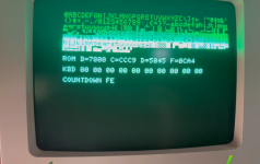
The original ROM is 2K.
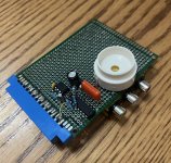
My PETTESTER is 2K.

The 27512 EPROM is 64K.

That means the 27512 EPROM can hold 32 off 2K ROM images.

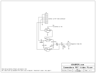
If you look at the schematic for the adapter, you should observe that the extra address lines (A11 through A15) are individually pulled HIGH via a resistor.

This means that the default address of the start of the 2K ROM image within the 27512 EPROM is 1111_1XXX_XXXX_XXXX = $F800.

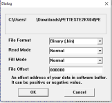
You set your EPROM programmer up to tell it that it is going to program a 27512 device - but (before you load the PETTESTER image) you also have to tell it there is an offset of F800 (hex) that the EPROM programmer has to apply BEFORE loading the binary image.

The EPROM programmer should, then, load the 2K PETTESTER binary image into the LAST 2K of the 27512 EPROM.

When you plug this into the adapter, address $F800 in the 27512 EPROM will magically become address $0000 relative to the adapter chip select (which is $E000) and everything should be good with the world!

Alternatively, and this will avoid all of this palaver, you could connect the unused address lines A11 through A15 (on the adapter board) to 0V instead, thus making the default 27512 offset 0000_0XXX_XXXX_XXX or $0000.

I hope this makes sense.

Dave
 

Oswald

Experienced Member
Joined
Mar 18, 2022
Messages
65
Aha! I set the write offset to $F800 and it worked! I'm getting a mem fail at 0 0 1C00 10 10.
 

daver2

10k Member
Joined
Jun 19, 2012
Messages
13,067
Location
UK - Worcester
Excellent.

Before we diagnose the memory fault, on the previous screen (where it checksums the ROMs) are the checksums stable or not?

There may be a ROM that is not stable, but that may not be fitted to your machine (in fact there will be no sockets for it).

Also (on the DRAM [sic] screen) is the amount of RAM found the same as is physically fitted to the machine?

Dave
 

Oswald

Experienced Member
Joined
Mar 18, 2022
Messages
65
This is what I see when I run the test. The DRAM test correctly reports 8k.
 

Attachments

  • Untitled4.png
    Untitled4.png
    587.7 KB · Views: 6
  • Untitled3.png
    Untitled3.png
    1 MB · Views: 6
  • Untitled2.png
    Untitled2.png
    915.2 KB · Views: 6
  • Untitled1.png
    Untitled1.png
    938.5 KB · Views: 6

Hutch

Experienced Member
Joined
Jul 1, 2018
Messages
293
Location
California
The Gs mean zero page is fine and the video ram looks fine.

On the screen with the countdown, do any of the ROM checksums change? 7800, CCC9, 5045 and 0CA4 every time you run it?

On that same screen, try pressing keys. The numbers after KBD should change but only one pair at a time.
 

Oswald

Experienced Member
Joined
Mar 18, 2022
Messages
65
Hi Hutch, the ROM checksums stay the same. Each key flipped only a single bit except space and return, but I assume that's because those are actually two separate keys under a single key cover? The keyboard issue I described earlier in the thread only appears sporadically now, for some reason, so it's entirely possible I just happened to catch the computer on a "good day". The next time it comes back I'll quickly swap in the EPROM and see what it reports.

The test also stalls after the DRAM test fails, is there anyway to bypass it manually?
 

daver2

10k Member
Joined
Jun 19, 2012
Messages
13,067
Location
UK - Worcester
>>> The test also stalls after the DRAM test fails, is there anyway to bypass it manually?

This is the last test in the sequence, so there is no point in bypassing it.

When you get to the DRAM test, is the address consistent every time it fails? Perform the test a few times and note down the result for each run. Adding a 'soft' reset button to the PET is usefull for this test to avoid constantly repowering the machine.

The test is identifying a faulty RAM (albeit a static RAM device rather than a 1 bit wide DRAM). The address of the fault is the key to identifying the faulty device in this case.

Dave
 
Top