Desperado
Veteran Member
- Joined
- Nov 25, 2017
- Messages
- 7,880
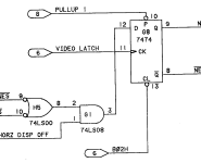
Ho guys i am here again for this 2001N pet. When i turn on i can see only a horizontal line on screen. I scoped video connector on board and i can see a waveform only on pin 5, horizontal signal. On pin 1 i have a 4,3V signal and 4,5V on pin 3.
View attachment IMG_20230105_104552.jpgView attachment IMG_20230104_203448.jpg
View attachment IMG_20230105_104552.jpgView attachment IMG_20230104_203448.jpg