• Please review our updated Terms and Rules here

Project to create an ATX 80286 mainboard based on the IBM 5170

modem7 thank you very much for your reply, it's helpful.

I read the experiment findings in the link you provided, that is very interesting information, I will remember this in my work later, it could prove useful.

In fact, as you pointed out, the symptoms I observed with the original IBM ROMs indeed gave similar findings as is described in this page when refreshing is manually turned off. Indeed after a variable amount of several seconds, the screen would also be blanked with a parity check error displayed.

Sometimes the period would last around 10-15 seconds, only just enough time to enter a 10 print "something"; 20 goto 10 program, run it and then the screen would blank and a parity check would appear at the top.

I should switch back to the IBM ROMs and probe the refresh logic from start to end to see if I can see something happen which corresponds with what happens on the screen. If I can't observe any refresh pulses or see the reset pulses being interrupted or erratic at any moment, it would be obvious to conclude that it's the refresh itself and not the parity checking mechanism. Thanks for pointing this out to me.

At the same time, I am still wondering, whatever the cause of the parity failures was before when only using the IBM BIOS, I did observe when using the generic MR BIOS that there was no problem using the mainboard for an extended period of time and no parity errors were happening at all during use of MS-DOS. Only when using a memory test in Checkit I was able to find some random parity errors in the test process reported by Checkit, and still no CPU stop event happened, the mainboard never halted the system at all. I could test the RAM for hours without any problems except to find occasional reporting of parity fails during the extended test sequences. The parity failures always would happen in a different memory area and then would keep occurring sequentially at that moment. I was getting the impression that this was not RAM area related but rather a random time moment where it would start to throw the parity errors and then keep doing that.

So the stability using the MR BIOS must have some reason for it. Perhaps there are checks in the code to verify the timer chip and reset it if needed, or something else happening in the background without any messages. Perhaps some sort of BIOS routine is acting similar as a refresh pulse on the RAMs, who knows...

Right now I am dealing with some urgent matters so I have cleared away the test setup and IBM mainboard. I restored all the original ICs as were present when I received it. As soon as I find a moment, maybe next weekend, I can resume testing and will do some probing with the scope. Having a properly matched schematic is really a huge advantage for me in this case.

Indeed, after your remarks and reading that page you linked, I feel it's better to start checking the refresh pulses through the whole circuit with a scope using the original IBM ROMs because they show parity faults much faster than when using the MR BIOS, just to observe if there is any interruption of refresh pulses happening.

The other test would be to disable parity checking entirely and then running an extended RAM test using checkit and MR BIOS. If the mainboard can run without errors for hours, that would be a clear indication that the memory control of the DRAM is not malfunctioning.

Thank you modem7, I really feel I want to make the determination whether something is failing in the refresh logic.

Also I should do more research on methods to try to remove the corroded outer layer of solder material the soldered pins in the affected areas.
I mean, resoldering is not so effective, and the corrosion seems to go into the component pins which makes them hard to solder after that anyway, so I expect that removing the solder and resoldering the ICs is not going to restore the solder joint quality to a proper state. Or maybe I can remove badly affected ICs and try to chemically treat them in some way, or polish the IC pins. The only other alternative would be to replace all the ICs. Some ICs are affected worse than others, even soldered vias have a corroded appearance in some areas. Later I will order a more delicate smooth tip for my desoldering iron which will not scratch the solder mask as easily as the standard shaped one.

I will do more testing as soon as I can find the time. I also want to first prepare a better quality ATX PSU and then exchange the wiring with AT wires and connectors. I just want to find a more precise 5V regulation and a more advanced PSU circuitry which will give me more confidence in the PSU. Perhaps I can put a series resistor between the POWER GOOD wire and the mainboard so I can short the POWER GOOD input at the mainboard side to ground for manual resetting of my test setup. I really do not like to need to power cycle these old PCBs so many times during testing when it's not really necessary.

Kind regards,

Rodney.
 
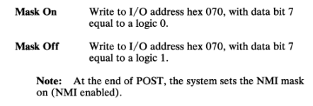
Additionally, I see what you mean when the testing software would disable the CPU from being able to receive an NMI. I think I should be able to see this happening in the logic. I think it's U127 replacing some outputs of the old 8255 "port B" used in XTs which would be turned off? Maybe the MR BIOS also does this automatically. I will check these outputs also when I do my next testing session just to be able to know what the mainboard is actually doing. I could add a LED or something for testing so I can monitor it.

Kind regards,

Rodney
 
Complicating the matter, with the background RAM refresh mechanism either faulty or disabled, the cells in a row of a RAM chip still get refreshed simply as the result of reading or writing any cell in that row.

1696301432660.png
 
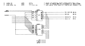
I think it's U127 replacing some outputs of the old 8255 "port B" used in XTs which would be turned off?
Yes, the circuit diagram and BIOS source code refers to it as 'Port B'.
U127 used for outputs. (Port B write.)
U128 used for inputs. (Port B read.)

I have it in the diagram at [here] as 'Port B'.

1696303331324.png
 
I also want to first prepare a better quality ATX PSU and then exchange the wiring with AT wires and connectors. I just want to find a more precise 5V regulation and a more advanced PSU circuitry which will give me more confidence in the PSU. Perhaps I can put a series resistor between the POWER GOOD wire and the mainboard so I can short the POWER GOOD input at the mainboard side to ground for manual resetting of my test setup. I really do not like to need to power cycle these old PCBs so many times during testing when it's not really necessary.
For when I have a 5160/5170 motherboard, with only video card, out on the table, I made what is pictured at [here]. Via large alligator clips, I connect it to a benchtop DC power supply (set to +5V). And you can see a reset button. The reset circuitry in the canister is shown at [here], although I think that I later increased the value of the resistor or capacitor.

Note: The lack of -5V/-12V/+12V is a problem in various scenarios.
 
Hi modem7,

That is super useful for my project, thanks a lot. I can use all information I can get, this is great stuff!
I made screenshots of your posts and saved them in my project folder.

I have not had to work with DRAMs much, but in this case it's really important to get the 5170 mainboard completely stable.
I really want to be thorough about it so it is not going to fail again.

I see what you mean with a benchtop power supply. That is really the most reliable method of applying power and has the additional benefit that you can monitor the current draw. You can have an expected default current value, and when powering up a known type of mainboard for testing, like in this case, you can anticipate the typical current and switch it off right away when something is out of spec. Then using a good ohm meter possibly the source can be found of any overcurrent happening.
When using a compatible video card which only needs 5V that would be a good idea. Like a old IBM one seems to be a good candidate. Or perhaps even using the most simple basic monochrome card just for the testing.

Your setup with the reset is similar to what I have in mind, indeed it's better to use an "own" reset timer circuit instead of relying on any PSU to provide it. And also a good idea to "box" the reset in plastic and make sure it can never accidentally touch anything. When troubleshooting it's always a good idea to make sure it's not needed to constantly watch everything on the desk for any short circuits. Thinking about this, I should make a plastic reset and PC speaker box with some power LEDs to signal power and reset action, that gives much more control and visual reference of what is happening with the system.

I am going to dispose of an old server case soon, maybe I can cut out some of the plating and back slot area with an angle grinder to see if I can make a desk stand to mount mainboards on. It depends on if after cutting, it can still be structurally strong enough for use. Using a stand can secure the whole thing with cards and protect any flexible component pins on the bottom from being bent. Also it's easier to keep everything together and set it aside for a moment when doing other things. Usually in a PC case it's too hard and awkward to probe pins.

I should have some server power supply somewhere here which is standard ATX form factor and made by Delta I think. It's pretty heavy and has not had many hours of operation or heavy loads. I can test it and then convert it to AT leads. That's my best option which I have in house at the moment.

I bought a typical PC power supply a few years ago for my projects not the cheapest but a reasonable price one, but after opening it and knowing how few components it has, I realise that I probably should soon switch to a better one, like a good brand such as Delta. These cheap powersupplies seem to lower the 5V rail somewhat when there is less load on the 12V, it's not ideal. If I find a good one which doesn't have such problems, I will report here in this thread about it.

I am also working on the complete 5170 type 2 schematic in Kicad which I will share with the community. I may also make a diagram PCB with all the component placements so it's easier to find any nets and component pins in a Kicad PCB layout screen. Later after I have everything I will make an attempt to organize the schematic more to be able to see the functional relations between parts more clearly. I am now working on sheet 10 so I'm about half way through.

I will keep the DRAM related parts on the bottom area of the schematic so I can create a new SRAM version later. I will provide 640K base memory and also add the UMB area of the D000 and E000 segments in the SRAMs. I will look at the AT memory map and try to provide more space in the ROMs so any option ROMS can be easily included in the same two chips. I should look at the memory area above 1MB as well to optionally feature it in SRAMs.

Kind regards,

Rodney
 
I have done some testing on the 5170 mainboard and the results are a bit strange.

The refresh function according to datasheets is being triggered through the /RAS line of the DRAMs.
The /RAS inputs of the 512K DRAM onboard on the type 3 mainboard is all controlled by the /RAS0 signal in the IBM schematic.

PROM U72 has the input REFRESH pulse on pin 18, and on its output D0 (pin6) there is the netname RRAS0.
This goes to latch U64 pin 3(IN) and pin 18(OUT) and becomes "RAM0_RAS".

RAM0_RAS drives U53 pin 3. U53 is also driven by /MEMR and /MEMW directly and delayed, this seems to be some kind of synchronization of RAS timing. On a scope it will make more sense of course.
U53 pin 6 finally generates output /RAS0 through a 30 ohms series resistor.

What I did was to connect my scope to the PCK parity detection signal, and let it wait for the signal to go high.
At the same time I sampled the /RAM0_RAS signal to monitor if there are any changes in the signal just before a parity error is thrown and the system halts. I did the tests using the original IBM BIOS which came with the mainboard. I could see the parity stop fault happen and the system halted. Each time I could see the PCK signal go high which signals a parity fault. Just before the parity fault I could not see the /RAM0_RAS stop delivering the RAS activity signal.

Right now I am having the "problem" that using the IBM BIOS apparently now I can't get a parity error anymore.
When I first started to test this IBM mainboard it threw parity errors after a few seconds. In this test session it took minutes to get the error using the IBM BIOS. Finally I am not getting any parity errors anymore since.

Things get even stranger, because I booted MS-DOS from XT-IDE (16 bit version) and ran Checkit 3 while monitoring the PCK line and the /RAM0_RAS line, however even when Checkit 3 was showing parity errors on the test screen (XX), the PCK line never got triggered even once. I checked, however the ENB_RAM_PCK line was always high, so parity checking was not disabled by Checkit while testing the RAM. I am not sure how Checkit can detect parity errors while the hardware parity error detection on the mainboard was not showing any errors. I don't think it's possible to read the parity byte from the parity DRAMs.

Right now I am running a simple basic program printing text on the screen and waiting for the parity errors from the IBM BIOS to appear however so far no errors. I will leave it running during the night.

I did borrow the RTC chip from my ARC mainboard because the one I was using didn't retain the BIOS setup.
After replacing it with the desoldered chip from the ARC mainboard I was able to keep the clock and settings using a 6V battery pack. I checked, the clock pulses to the RTC keep going during power off.
I will need to order some more RTC chips since I only have one working chip now apparently.
With the IBM BIOS I am using GSETUP.EXE. It's a little strange because memory size is set to 512k but only showing 511k of RAM in MEMSIZE and also in Checkit.

It's weird that Checkit 3 is showing parity errors occasionally while the hardware parity error detection system is not initiating this error since it is not triggered at all. So Checkit must conclude the parity errors by itself or it may be a software malfunction of Checkit. I have tested with Checkit using the original IBM BIOS.

I'm not getting any conclusive results and the test results I have seen are not consistent throughout the time period during which I have tested the mainboard.

I want to test more stuff but the IBM mainboard is a little limited with only 512KB.
I think I will look at removing the DRAM and inserting SRAM with a new memory decoder, for example using 512KB for the low byte and 512KB for the high byte. This way I can cover the 1MB region for the first 640KB and UMBs.

Also I need to read out the PALs and PROMs from the 5170 to try to document the logic equations.
I am using the AT PSU for the moment and it keeps delivering a proper 5V level.
Later this weekend I will convert a better ATX PSU for testing.

Perhaps I am dealing with some bad solder joints or something, it is not looking like a faulty component.
I will reflow all the pins on the IBM mainboard, and then do some more testing.
Soon I will wire up an adapter socket for reading out the PALs as a ROM chip which code I will be trying to convert to logic equations using software.

I think reading the PROM code should be more straight forward, I will try it as well.

Kind regards,

Rodney
 
I just tested with basic only using the IBM BIOS and after a long time I got another parity check 1 message with ????? location unknown. So the problem is of course still present just harder to detect.

I will let Checkit run overnight and monitor the PCK line and refresh pulses.

Kind regards,

Rodney
 
I just tried Checkit again while the problem had worsened, and indeed now it was able to trigger my scope with the PCK signal. So maybe before my cheap scope didn't catch the PCK signal.

So apparently the parity errors are coming from the PCK after all.
Just probably they were too short pulses because they were not triggering a system halt through NMI.

While trying to boot MS-DOS I was also getting parity errors from the IBM BIOS.
After a few attempts I was able to boot and start Checkit.
I already cought 2 PCK events with the single trigger function of my scope.

I will keep investigating this problem.
Maybe I should replace some of the parity detect logic, it may be marginal.
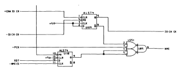
For example also U85 the LS51 whose output is involved in generating the PCK signal.
Did anyone here ever see a faulty PCK detection happen before?
I suppose that U6, U12, U85, U59 are some of the candidates for replacement.
And I see a lot of reflowing in my future.

I am also working on the ARC X286 Model 12, I have replaced the CPU socket with a PLCC socket, I want to try a newer and faster Harris CPU on this mainboard, which generates less heat and doesn't need any cooling.
I will test the ARC mainboard this weekend as well, let's hope I'm lucky that it's fully working.
There is 1MB onboard RAM on this mainboard and it's running at 12,5 Mhz.
I could be able to test the PALs from the other ARC mainboard, if I have two stable sets that would be great for my project.

Kind regards,

Rodney
 
By the way, if someone knows a method to adapt the DS12885 to replace the 146818 RTC, I would appreciate to know how you did it. There are some differences, I am still trying to understand the appnotes about this what needs to be done actually to get a DS12885 to work.

Kind regards,

Rodney
 
I am using the AT PSU for the moment and it keeps delivering a proper 5V level.
Measured via a multimeter or oscilloscope? Imagine glitches, something a multimeter isn't expected to detect.

Later this weekend I will convert a better ATX PSU for testing.
Yes, it would be good to rule out the PSU.

By the way, if someone knows a method to adapt the DS12885 to replace the 146818 RTC, I would appreciate to know how you did it. There are some differences, I am still trying to understand the appnotes about this what needs to be done actually to get a DS12885 to work.
The DS12885/DS12887/DS12C887 datasheet at [here] contains, "Drop-In Replacement for IBM AT Computer Clock/Calendar".
Is there a particular reason that you think the DS12885 will not work as it is in the IBM AT ?
 
Hi modem7,

Thanks for your replies. It's a good point, I have looked at the VCC with a scope but not monitored it for an extended period. I will try to use the scope trigger on a sensitive AC setting during another RAM test to try to detect some kind of power glitch.

I have tested with two powersupplies, one is a modified modern ATX powersupply which has a slightly low 5V rail, the other is the original AT power supply from late 80s. The AT powersupply has some problem to start up, sometimes I need to try a few times to get it going. The caps are all fine I have taken them out and tested them. So indeed I will soon try to find the better quality server powersupply which I have here somewhere and modify it for the project.

About the RTC, before I also had the same thought, these RTC ICs are so similar. However in my experience the DS12885 cannot be a drop-in exchange for the 146818. After simply exchanging the IC it doesn't work. I bought a number of salvaged DS12885 from Aliexpress a while ago, but they cannot run in any AT mainboards I have tested. They all have slightly different markings which look old so it doesn't appear that these are fakes.

I do know that there was some documentation made by Dallas which shows the differences between them and mentions modifications. I attached the document in this post. The DS12885 seems to need a crystal rather than an external oscillator, that is the major difference. I am not fully done experimenting with this yet. Possibly if I connect the external clock with both opposite phases to both the X1 and X2 inputs, the DS12885 may be able to function after all as a replacement. I will experiment more with this later because I do have some DS12885 RTCs.

The DS12885 has Motorola or Intel timing modes, which default to Intel with an internal pull-down on pin 1 according to the datasheet. However I have also seen mainboards where they have wired pin 1 to ground as a modification to the PCB, so possibly there are some issues with this.

Kind regards,

Rodney
 

Attachments

  • 146818 RTC replace by DS12885 app521.pdf
    29.5 KB · Views: 5
Last edited:
About the RTC, before I also had the same thought, these RTC ICs are so similar. However in my experience the DS12885 cannot be a drop-in exchange for the 146818. ...
Correct. Not even Dallas or Maxim claims that it is a drop-in-replacement for the 146818. (I.e. drop-in-replacement for the 146818 globally, in all computers that use the 146818.)

But in the specific case of a 146818 in an IBM AT, they do say that the DS12885 is a drop-in-replacement. They would have looked at how the 146818 is used in the IBM AT, made the assessment, and probably did an actual test before declaring "Drop-In Replacement for IBM AT Computer Clock/Calendar" in the datasheet.

The datasheet that you attached contains the statement, "The DS12885 is designed to work with a 32.768 kHz crystal connected directly to pins 2 and 3." But I do not see the word "only" between "designed" and "to". I think, through poor wording, that the author intended to describe one possibility. That is supported by the document at [here], which, in the X1/X2 row of the pin description section, contains, "Pin X1 is the input to the oscillator and can optionally be connected to an external 32.768kHz oscillator. The output of the internal oscillator, pin X2, is left unconnected if an external oscillator is connected to pin X1."
 
Hi modem7,

Thanks for checking the datasheet exact wordings for the 12885. What you write makes sense from the language in the datasheet however I could not get the DS12885 chips I have to function in place of the 146818, I tested with the NCR PC-8 and ARC X286 Model 12.

There is the possibility that the ICs I received from China are all defective, otherwise I can't think of any other logical reason. It felt strange to me that it's claimed to be a replacement yet not working, that seemed counter productive. Before in my XT revision 1 design I integrated and tested these DS12885 and I could not get them to work. Perhaps they are indeed all bad, that is possible. I am starting to think this is the case. It's great to talk with you about this, thanks.

I finished modifying a Delta powersupply and it has good stable 5V and all other voltages, I replaced one capacitor for the 5V rail which was worn out, the rest are fine. This particular Delta powersupply is from a HP PC, but I am sure I have a "heavier" version somewhere from a server. Anyway, this 300W one looks to be of good quality.

I have done more testing but unfortunately still no luck, the parity errors still persisted so I am looking at other possible causes.

I have reflowed the CPU socket and all DRAM sockets, and tried to replace U85, a 74LS51, however both replacements I tried from other mainboards give a 107 System board error, that refers to the Hot NMI Test I saw on your website. When replacing the original one in the socket, no error 107 anymore. I will try to order some new 74LS51 replacements.

I also replaced the Time delay IC U61 just to have a try and see what happens since it looks like a DRAM critical part, and now testing with Checkit again.

I will continue to try to replace ICs which are involved in the parity detection and inserting sockets. After that if it's still not solved I will look at the ICs involved in refresh.

It seems that the parity errors are only appearing after having tested for a while now. When I start the test, everything looks fine however minutes later there are suddenly parity errors appearing. Possibly there is a problem and resulting failure when a certain component warms up.

Anyway, I appreciate your time modem7 and thanks for following my posts. I hope I can finally fix the problems because I want to repair this 5170 mainboard. If it's any other brand I can care less but this is my only IBM 286 mainboard.

Unfortunately many ICs are not in my parts supply(ALS types and 74LS51 etc) so I can only get them from my other mainboards, which has the added problem of shorter legs on these ICs. I tried with the 74LS51 to solder it into a precision IC socket to ensure a solid connection into the socket however I still got the 107 error even when using a socket inbetween for the stronger connection.

If all repairs fail to fix the problem, I may revert to disabling the parity logic. I won't be needing it and I can do extensive RAM testing to make sure the mainboard works properly otherwise. Anyway, I am not there yet to consider this course of action because I still hope to have a functional 5170 board in a complete original component and functional state.

So far this parity error is strange and rather unpredictable when it will happen. These types of errors which are rare and intermittent to happen are really hard to trace so I may resort to replacing various ICs which look like they could be involved from the schematic, and see if I can trace the fault. Unfortunately each attempt now takes up to 30 minutes to know whether it has fixed the issue.

By the way, do you think that the problem could lie in the tantalum caps? For example if they cause some intermittent current spikes on the supply rails? I will also replace these caps in the next desoldering session as soon as I have seen any parity errors again on this testing session.

Kind regards,

Rodney
 
Last edited:
I have not yet found the cause of the parity check errors on my 5170 mainboard.

- I have replaced all the tantalum capacitors
- I have replaced the sockets with spring types which seem to hold ICs with shorter legs better. At least, the precision types I have are not great either, they don't feel tight when inserting an IC, so the spring types I have are preferable for me at the moment. I took them from another mainboard.

- I have tested with another 74LS51 which I took from another mainboard. However I am also getting the 107 error with this IC so it appears that there is a timing difference between different brands of 74LS51 ICs.

Mitsubishi M74LS51P: not working properly as U85 on my mainboard, causes error 107 Hot NMI test
Motorola SN74LS51N: not working properly as U85 on my mainboard, causes error 107 Hot NMI test
Signetics 74LS51N(1986) does not normally cause the error 107, only perhaps three times during all my tests.
Unfortulately I don't have other ones to test with. If I find any, I will try them.

I will test more after replacing some other ICs in the parity check and refresh circuits now. To save some time I will replace them in groups.

Kind regards,

Rodney
 
Since it looks like repairing the 5170 mainboard will take more time, I looked at the ARC mainboard first to see what state it is in.

It is showing the effects of battery chemicals in the area around the battery connector, near the keyboard connector. Some of the jumpers were almost fused to their headers and required pliers to get them off. I replaced those headers. I soldered in a PLCC socket and inserted a Harris 16Mhz 286 plastic CPU.

I tested with the generic 286 MR BIOS, which gave me the LH-LLLL beep code which signals a problem in RAM bank 0. Unfortunately this bank was factory soldered into the mainboard so I proceeded to desolder 18 41256 DRAMs, desoldered 18 IC sockets from another mainboard and soldered them into the ARC mainboard. Which took a while. After placing a different set of DRAMs, the ARC mainboard POSTed correctly. I put DRAMs into the second 512KB sockets and tested again, the mainboard now has 1MB of DRAM onboard, which is mapped in the 640Kb region and the rest is mapped as extended memory above the 1MB memory area. There are several jumpers onboard which are "unexplained" which might be related to wait states or memory mapping, and possibly could modify memory allocation etc., I will look into this later. I left Checkit testing during the night and it didn't report any RAM faults. At least I have confirmed that the ARC is fully functional, good news!

I will desolder all the ICs in the area affected by battery chemicals, and resolder them after treating the ARC mainboard with acid another time. Also I will remove the solder from the affected via holes and AT power connectors, and resolder those after acid treatment. After all that I will have more solid confidence in this ARC mainboard. I must say, I love their product, it appears really solid and proper PC level reliable. First I will return to repairing the 5170 mainboard now.

I will desolder all ICs from the 5170 in groups, solder in IC sockets and replace each group. I will take photos of the exact IC types in which sockets they are, and then mark the original ICs before replacing them for testing. I am taking the thorough option because I need to determine the cause of the parity faults.

Of course, there is the possibility of other problems such as a broken trace which becomes apparent through heat expansion in the back of my mind. In that case I will rethink the whole matter of whether I want to continue with this 5170 mainboard. It does seem that this mainboard suffered from extended periods of exposure to very moist air. I may replace the CPU later if all else fails.

I will post here what my findings are from the desoldering and replacement work of groups of ICs according to their function. I will start with the parity logic, then refresh control logic, RAS/CAS logic and DRAM multiplexer ICs.
Somehow I have a feeling this search might not result in success, but I will try it anyway to exclude things, and I still have some hope I can finally report a working 5170 mainboard for my project.

Kind regards,

Rodney
 
I have replaced:

5170 PARITY error detect logic
====================

- U6 74F280
- U12 74F280
- U59 74F08
- U86 74F74
- U121 74ALS04
- U127 74ALS175
- U128 74ALS244

It's not all the logic involved but some of the major components. Replacing U85 has not been successful because of timing differences between different brands of 74LS51.

I have turned on another Checkit RAM test which is now running for 80 minutes. So far I have not seen any parity errors reported -yet- so possibly the problem may be solved now. I will do more testing overnight. If I still find more problems I will replace the next group of logic and post here.

I hope I can have two reference mainboards for my project now.

I have been working on the ARC X286 Model 12 mainboard to deal with the worst of the battery chemical damage, this makes many solder joints really hard to reflow. I am trying to clean again and scrub off the hardened solder, however it seems that I will need more acid cleaning because there is still something contaminating the solder joints coming off the PCB holes and vias. I will try "flossing" the vias and other holes with some copper wire and acid.

Kind regards,

Rodney
 
Mitsubishi M74LS51P: not working properly as U85 on my mainboard, causes error 107 Hot NMI test
Motorola SN74LS51N: not working properly as U85 on my mainboard, causes error 107 Hot NMI test
Signetics 74LS51N(1986) does not normally cause the error 107, only perhaps three times during all my tests.
Unfortunately I don't have other ones to test with. If I find any, I will try them.
Replacing U85 has not been successful because of timing differences between different brands of 74LS51.
I just now, pulled out two spare IBM 5170 motherboards of mine.
On one, a type 1 motherboard, U85 is a Texas Instruments SN74LS51N.
On the other, a type 3 motherboard, U85 is a Texas Instruments SN74LS51N.

I would have thought that if timing here was critical, i.e. affected by make of IC, that the engineers would have put in an ALS, not LS.
 
Hi modem7,

I don't have any TI 74LS51N here unfortunately.
Since these are used on your 5170s, thanks for checking that by the way, they are certain to be suitable, from that same manufacturing period by TI.

I will try to order more 74LS51 from Aliexpress, maybe I can find a TI one.
I will check my Taiwanese turbo XT, maybe that one has some TI ICs.

In fact, things are much more subtle. To reach the proper timing, it will be needed in certain circuits to use a faster or slower chip, so both ways may apply depending on what's needed in a particular circuit. Manufacturers of these systems already did the testing and determinations of choices of logic. The XT and AT are delicate in their timing, and doing a discrete design will pose some challenges in those areas. Add DRAM to the mix and it's even more complicated I am certain. Thankfully I won't be doing that.

Different combinations in critical circuits will have different results which may or may not work. Changing one IC on one end may for example change all the timing and require also changing other ICs in a system. It's the challenge to make the right combinations. Which is why we see a variety of logic family types in these discrete chipset PCs, much of this is deliberate. I have a lot of experience with this matter after debugging prototype mainboards and interfaces I have designed and built. Using CPLD or FPGA, it is much easier to adjust the timing than with TTL ICs.

If anyone for example is having trouble with an XT-IDE PCB they are assembling themselves to get it working to control the 16 bit IDE bus using an XT, they should look at the control timing ICs and test with different types, and changing to more or less delay for example. I made my own variation of this interface, the same issue needed to be dealth with. Some ICs need to be slower, others faster, and a certain combination will work best. After determining the logic types, from then on it's easy to reproduce the interface in a good working condition. The same probably applies to the 16 to 8 bit databus conversion in the IBM AT which I am sure is also very sensitive. I will get acquainted with this very soon in my prototypes I am sure, I am already anticipating this kind of difficulties.

In order to determine which logic will work in certain circuits, testing in the circuit in question will be required first.
If I had some 74ALS51 I could experiment with these and see what happens.

I won't be using any 74LS51 in my new 286 design. Especially after I have seen the different results from different manufacturers in my 5170. I prefer more generic logic ICs.
I prefer TI and Philips actually if I have the choice and I need faster ICs in certain circuits.

Since the 5170 appears stable now I will not do further modifications in the DRAM circuits since that will be unnecessary and probably counter productive, I will be replacing all these in my new design with SRAM.

I will be designing a custom memory PCB which includes all RAM and ROM and new memory decoding logic to make conventional RAM, UMBs and extended RAM areas. And a larger ROM area will be available by default, possibly page selectable by switch or jumper, which will enable the user to choose different BIOS software if desired. I will insert this PCB into the 5170 circuits so I will be desoldering everything I won't be needing and putting in sockets for testing the new memory system. I will put the DRAM and ICs back to original later when I am done testing. Probably I will be using MR-BIOS for testing with my new design.

My ARC mainboard does have extended battery chemical damage. This has weakened many trace connections. I cleaned a small test area and repaired the traces where it was apparently needed, later I will be desoldering, cleaning and repairing some other corroded PCB areas.

Kind regards,

Rodney
 
Back
Top