I have looked at the contents of the JED files found in the mame download as Sergey pointed out.
I wanted to see if I can create some equations which can be used in a schematic representation of the PAL16L8 chips on the 5170 mainboard.
However something is not as I expected in these files.
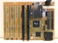
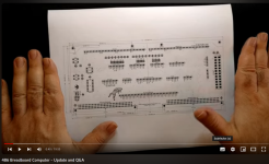
U87 in the IBM 5170 schematics is a key component for buffer control and DMA control.
In the IBM schematic it is shown as having 13 inputs and 5 outputs.
So we would expect to see something along those lines as inputs and outputs.
When looking at the U87 JED file which should represent a PAL16L8, I am seeing this:
JEDEC file generated by BP-1200/48/SM48D from PAL14L4 02/13/11 21:27:38*
DM MMI(AMD)*
DD PAL14L4*
QF448*
G0*
F0*
L00000 0000000000000000000000000000*
L00028 0000000000000000000000000000*
L00056 0000000000000000000000000000*
L00084 0000000000000000000000000000*
L00112 0000000000000000101010100000*
L00140 0000000000000000101010100000*
L00168 0000000000000000000000000000*
L00196 0000000000000000000000000000*
L00224 0000000000000000000010100000*
L00252 0000000000000000000010100000*
L00280 0000000000000000000010100000*
L00308 0000000000000000000010100000*
L00336 0000000000000000101010100000*
L00364 0000000000000000101010100000*
L00392 0000000000000000101010100000*
L00420 0000000000000000101010100000*
C02A8*
8B9A
The JED file contains a reference to a PAL14L4 part, which can't match with the IBM schematic as you would expect..
Since the schematic has 5 outputs that we need the logic equations for.
I tried the OPALJR JED2EQN which results in this:
; JED2EQN -- JEDEC file to Boolean Equations disassembler (Version V063)
; Copyright (c) National Semiconductor Corporation 1990-1993
; Disassembled from U87.JED. Date: 7-28-123
chip U87 PAL14L4
i1=1 i2=2 i3=3 i4=4 i5=5 i6=6 i7=7 i8=8 i9=9 GND=10 i11=11 i12=12
i13=13 o14=14 o15=15 o16=16 i18=18 i19=19 VCC=20
equations
/o16 = i2 * /i2 * i1 * /i1 * i3 * /i3 * i19 * /i19 * i4 * /i4 * i18 * /i18
* i5 * /i5 * i6 * /i6 * /i7 * /i13 * /i8 * /i12 * i9 * /i9 * i11
* /i11
+ i2 * /i2 * i1 * /i1 * i3 * /i3 * i19 * /i19 * i4 * /i4 * i18 * /i18
* i5 * /i5 * i6 * /i6 * /i7 * /i13 * /i8 * /i12 * i9 * /i9 * i11
* /i11
/o15 = i2 * /i2 * i1 * /i1 * i3 * /i3 * i19 * /i19 * i4 * /i4 * i18 * /i18
* i5 * /i5 * i6 * /i6 * i7 * /i7 * i13 * /i13 * /i8 * /i12 * i9
* /i9 * i11 * /i11
+ i2 * /i2 * i1 * /i1 * i3 * /i3 * i19 * /i19 * i4 * /i4 * i18 * /i18
* i5 * /i5 * i6 * /i6 * i7 * /i7 * i13 * /i13 * /i8 * /i12 * i9
* /i9 * i11 * /i11
+ i2 * /i2 * i1 * /i1 * i3 * /i3 * i19 * /i19 * i4 * /i4 * i18 * /i18
* i5 * /i5 * i6 * /i6 * i7 * /i7 * i13 * /i13 * /i8 * /i12 * i9
* /i9 * i11 * /i11
+ i2 * /i2 * i1 * /i1 * i3 * /i3 * i19 * /i19 * i4 * /i4 * i18 * /i18
* i5 * /i5 * i6 * /i6 * i7 * /i7 * i13 * /i13 * /i8 * /i12 * i9
* /i9 * i11 * /i11
/o14 = i2 * /i2 * i1 * /i1 * i3 * /i3 * i19 * /i19 * i4 * /i4 * i18 * /i18
* i5 * /i5 * i6 * /i6 * /i7 * /i13 * /i8 * /i12 * i9 * /i9 * i11
* /i11
+ i2 * /i2 * i1 * /i1 * i3 * /i3 * i19 * /i19 * i4 * /i4 * i18 * /i18
* i5 * /i5 * i6 * /i6 * /i7 * /i13 * /i8 * /i12 * i9 * /i9 * i11
* /i11
+ i2 * /i2 * i1 * /i1 * i3 * /i3 * i19 * /i19 * i4 * /i4 * i18 * /i18
* i5 * /i5 * i6 * /i6 * /i7 * /i13 * /i8 * /i12 * i9 * /i9 * i11
* /i11
+ i2 * /i2 * i1 * /i1 * i3 * /i3 * i19 * /i19 * i4 * /i4 * i18 * /i18
* i5 * /i5 * i6 * /i6 * /i7 * /i13 * /i8 * /i12 * i9 * /i9 * i11
* /i11
Where I am seeing only 3 outputs instead of 5 outputs.
There is another matter which can't be right, in the U130 JED file, also a PAL16L8 part,
I am seeing this:
JEDEC file generated by BP-1200/48/SM48D from PAL14L4 02/13/11 23:50:18*
DM MMI(AMD)*
DD PAL14L4*
QF448*
G0*
F0*
L00000 0000000000000000000000000000*
L00028 0000000000000000000000000000*
L00056 0000000000000000000000000000*
L00084 0000000000000000000000000000*
L00112 1111111111111111111111111111*
L00140 1111111111111111111111111111*
L00168 1111111111111111111111111111*
L00196 1111111111111111111111111111*
L00224 1111111111111111111111111111*
L00252 1111111111111111111111111111*
L00280 1111111111111111111111111111*
L00308 1111111111111111111111111111*
L00336 1111111111111111111111111111*
L00364 1111111111111111111111111111*
L00392 1111111111111111111111111111*
L00420 1111111111111111111111111111*
C29D6*
8CD0
This doesn't look right either.
From the resulting EQN file it's apparent that this also cannot be correct to represent the part on the 5170 mainboard:
; JED2EQN -- JEDEC file to Boolean Equations disassembler (Version V063)
; Copyright (c) National Semiconductor Corporation 1990-1993
; Disassembled from U130.JED. Date: 7-28-123
chip U130 PAL14L4
GND=10 o14=14 o15=15 o16=16 VCC=20
equations
/o16 = vcc
+ vcc
+ vcc
+ vcc
/o15 = vcc
+ vcc
+ vcc
+ vcc
/o14 = vcc
+ vcc
+ vcc
+ vcc
I don't know why these JED files are specified in this manner, but I can't rule out that this is perhaps specific for emulation purposes only.
I will spend some more time searching for other information about the 2 PAL16L8 contents equations, maybe I can find them somewhere.
Additionally, I have indeed seen this information confirmed in some PAL16L8 datasheets, there is a mention of a retention time of ">20 years".
This doesn't indicate exactly how long the theoretical retention is, but it does make me ask myself if perhaps these old PAL chips are going to fail eventually.
Perhaps that's exactly what happened with my ARC mainboard which suddenly stopped functioning reliably after a sudden power drop when I accidentally shorted VCC to GND on a pinheader.
The power supply when into protection mode, but after I turned it off and back on, there was a big stability problem in hardware detection on the ISA bus.
Kind regards,
Rodney
I wanted to see if I can create some equations which can be used in a schematic representation of the PAL16L8 chips on the 5170 mainboard.
However something is not as I expected in these files.
U87 in the IBM 5170 schematics is a key component for buffer control and DMA control.
In the IBM schematic it is shown as having 13 inputs and 5 outputs.
So we would expect to see something along those lines as inputs and outputs.
When looking at the U87 JED file which should represent a PAL16L8, I am seeing this:
JEDEC file generated by BP-1200/48/SM48D from PAL14L4 02/13/11 21:27:38*
DM MMI(AMD)*
DD PAL14L4*
QF448*
G0*
F0*
L00000 0000000000000000000000000000*
L00028 0000000000000000000000000000*
L00056 0000000000000000000000000000*
L00084 0000000000000000000000000000*
L00112 0000000000000000101010100000*
L00140 0000000000000000101010100000*
L00168 0000000000000000000000000000*
L00196 0000000000000000000000000000*
L00224 0000000000000000000010100000*
L00252 0000000000000000000010100000*
L00280 0000000000000000000010100000*
L00308 0000000000000000000010100000*
L00336 0000000000000000101010100000*
L00364 0000000000000000101010100000*
L00392 0000000000000000101010100000*
L00420 0000000000000000101010100000*
C02A8*
8B9A
The JED file contains a reference to a PAL14L4 part, which can't match with the IBM schematic as you would expect..
Since the schematic has 5 outputs that we need the logic equations for.
I tried the OPALJR JED2EQN which results in this:
; JED2EQN -- JEDEC file to Boolean Equations disassembler (Version V063)
; Copyright (c) National Semiconductor Corporation 1990-1993
; Disassembled from U87.JED. Date: 7-28-123
chip U87 PAL14L4
i1=1 i2=2 i3=3 i4=4 i5=5 i6=6 i7=7 i8=8 i9=9 GND=10 i11=11 i12=12
i13=13 o14=14 o15=15 o16=16 i18=18 i19=19 VCC=20
equations
/o16 = i2 * /i2 * i1 * /i1 * i3 * /i3 * i19 * /i19 * i4 * /i4 * i18 * /i18
* i5 * /i5 * i6 * /i6 * /i7 * /i13 * /i8 * /i12 * i9 * /i9 * i11
* /i11
+ i2 * /i2 * i1 * /i1 * i3 * /i3 * i19 * /i19 * i4 * /i4 * i18 * /i18
* i5 * /i5 * i6 * /i6 * /i7 * /i13 * /i8 * /i12 * i9 * /i9 * i11
* /i11
/o15 = i2 * /i2 * i1 * /i1 * i3 * /i3 * i19 * /i19 * i4 * /i4 * i18 * /i18
* i5 * /i5 * i6 * /i6 * i7 * /i7 * i13 * /i13 * /i8 * /i12 * i9
* /i9 * i11 * /i11
+ i2 * /i2 * i1 * /i1 * i3 * /i3 * i19 * /i19 * i4 * /i4 * i18 * /i18
* i5 * /i5 * i6 * /i6 * i7 * /i7 * i13 * /i13 * /i8 * /i12 * i9
* /i9 * i11 * /i11
+ i2 * /i2 * i1 * /i1 * i3 * /i3 * i19 * /i19 * i4 * /i4 * i18 * /i18
* i5 * /i5 * i6 * /i6 * i7 * /i7 * i13 * /i13 * /i8 * /i12 * i9
* /i9 * i11 * /i11
+ i2 * /i2 * i1 * /i1 * i3 * /i3 * i19 * /i19 * i4 * /i4 * i18 * /i18
* i5 * /i5 * i6 * /i6 * i7 * /i7 * i13 * /i13 * /i8 * /i12 * i9
* /i9 * i11 * /i11
/o14 = i2 * /i2 * i1 * /i1 * i3 * /i3 * i19 * /i19 * i4 * /i4 * i18 * /i18
* i5 * /i5 * i6 * /i6 * /i7 * /i13 * /i8 * /i12 * i9 * /i9 * i11
* /i11
+ i2 * /i2 * i1 * /i1 * i3 * /i3 * i19 * /i19 * i4 * /i4 * i18 * /i18
* i5 * /i5 * i6 * /i6 * /i7 * /i13 * /i8 * /i12 * i9 * /i9 * i11
* /i11
+ i2 * /i2 * i1 * /i1 * i3 * /i3 * i19 * /i19 * i4 * /i4 * i18 * /i18
* i5 * /i5 * i6 * /i6 * /i7 * /i13 * /i8 * /i12 * i9 * /i9 * i11
* /i11
+ i2 * /i2 * i1 * /i1 * i3 * /i3 * i19 * /i19 * i4 * /i4 * i18 * /i18
* i5 * /i5 * i6 * /i6 * /i7 * /i13 * /i8 * /i12 * i9 * /i9 * i11
* /i11
Where I am seeing only 3 outputs instead of 5 outputs.
There is another matter which can't be right, in the U130 JED file, also a PAL16L8 part,
I am seeing this:
JEDEC file generated by BP-1200/48/SM48D from PAL14L4 02/13/11 23:50:18*
DM MMI(AMD)*
DD PAL14L4*
QF448*
G0*
F0*
L00000 0000000000000000000000000000*
L00028 0000000000000000000000000000*
L00056 0000000000000000000000000000*
L00084 0000000000000000000000000000*
L00112 1111111111111111111111111111*
L00140 1111111111111111111111111111*
L00168 1111111111111111111111111111*
L00196 1111111111111111111111111111*
L00224 1111111111111111111111111111*
L00252 1111111111111111111111111111*
L00280 1111111111111111111111111111*
L00308 1111111111111111111111111111*
L00336 1111111111111111111111111111*
L00364 1111111111111111111111111111*
L00392 1111111111111111111111111111*
L00420 1111111111111111111111111111*
C29D6*
8CD0
This doesn't look right either.
From the resulting EQN file it's apparent that this also cannot be correct to represent the part on the 5170 mainboard:
; JED2EQN -- JEDEC file to Boolean Equations disassembler (Version V063)
; Copyright (c) National Semiconductor Corporation 1990-1993
; Disassembled from U130.JED. Date: 7-28-123
chip U130 PAL14L4
GND=10 o14=14 o15=15 o16=16 VCC=20
equations
/o16 = vcc
+ vcc
+ vcc
+ vcc
/o15 = vcc
+ vcc
+ vcc
+ vcc
/o14 = vcc
+ vcc
+ vcc
+ vcc
I don't know why these JED files are specified in this manner, but I can't rule out that this is perhaps specific for emulation purposes only.
I will spend some more time searching for other information about the 2 PAL16L8 contents equations, maybe I can find them somewhere.
Additionally, I have indeed seen this information confirmed in some PAL16L8 datasheets, there is a mention of a retention time of ">20 years".
This doesn't indicate exactly how long the theoretical retention is, but it does make me ask myself if perhaps these old PAL chips are going to fail eventually.
Perhaps that's exactly what happened with my ARC mainboard which suddenly stopped functioning reliably after a sudden power drop when I accidentally shorted VCC to GND on a pinheader.
The power supply when into protection mode, but after I turned it off and back on, there was a big stability problem in hardware detection on the ISA bus.
Kind regards,
Rodney

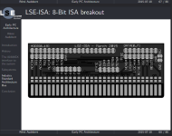
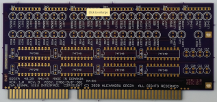
") ) not needed a breakout PCB yet, because I take a long time to prepare and examine the circuits first. However it does seem handy to have one. Especially to have some useful and accessible pin connectors for securely attaching scope probes would be useful indeed, and the corresponding ground connection terminals for example for an alligator clip. And a lot of ground plane for solid measurements. And perhaps adding a POST code display, and even a second ISA slot on top for plugging in a card which you can then easily probe when it's sticking out of the PC case. I have seen this method being used on some very old mini computer systems(which I love!) where he probed and checked a drive interface card outside the case. Alexandru's card is the most cool one! However many signals may not be possible to monitor them by vision. It just looks cool though!
) not needed a breakout PCB yet, because I take a long time to prepare and examine the circuits first. However it does seem handy to have one. Especially to have some useful and accessible pin connectors for securely attaching scope probes would be useful indeed, and the corresponding ground connection terminals for example for an alligator clip. And a lot of ground plane for solid measurements. And perhaps adding a POST code display, and even a second ISA slot on top for plugging in a card which you can then easily probe when it's sticking out of the PC case. I have seen this method being used on some very old mini computer systems(which I love!) where he probed and checked a drive interface card outside the case. Alexandru's card is the most cool one! However many signals may not be possible to monitor them by vision. It just looks cool though!