| VCF West | Aug 01 - 02 2025, | CHM, Mountain View, CA |
| VCF Midwest | Sep 13 - 14 2025, | Schaumburg, IL |
| VCF Montreal | Jan 24 - 25, 2026, | RMC Saint Jean, Montreal, Canada |
| VCF SoCal | Feb 14 - 15, 2026, | Hotel Fera, Orange CA |
| VCF Southwest | May 29 - 31, 2026, | Westin Dallas Fort Worth Airport |
| VCF Southeast | June, 2026 | Atlanta, GA |
-
Please review our updated Terms and Rules here
You are using an out of date browser. It may not display this or other websites correctly.
You should upgrade or use an alternative browser.
You should upgrade or use an alternative browser.
Schematic diagrams and best practices
- Thread starter tech58761
- Start date
cj7hawk
Veteran Member
And Hydrogen Peroxide... I am curious also.Sulfuric, ammonia, and HF? Sheesh...mind if I ask what the machine is?
Rocket motor controller for a Saturn 5 engine tester? I have no idea.
Anyway the schematics look nice - Maybe add a block diagram?
I am not sure of any specific best practice for schematics, but they rarely come alone - generally there's some block diagrams that describe the key elements in the circuit and accompanying text that describes the operation of the circuit, and a BOM, identifying which diagram they are on, and often a list of diagrams.
I'm not suggesting that's best practice - just what I'd observe I see in other schematics when produced.
I've noticed some IC numbers (eg, u9) are repeated on multiple pages, so changing those to a board location reference, and if there's no references on the boards, just include a set of photos of the boards with a reference grid overlaid.
Well, hope that helps -
") As schematics go, any information is better than no information.
As schematics go, any information is better than no information. tech58761
Experienced Member
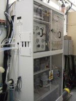
Yes, it definitely handles some serious chemicals don't it?! And some of these boards definitely show evidence of fumes getting into the works!
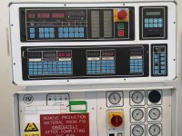
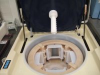
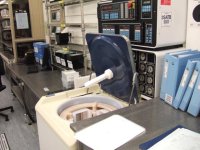
This is the controller for the FSI 'Saturn' wafer processor system. (which makes part of cj7hawk's post ironic)
I used to work on the various boards in this system and recently got a wild hair to get this system documented as to all the circuit boards etc.
I even found an already scanned copy of the operator's manual and a physical copy the tech book (blueprints etc. of all the major components) which I did scan as well.
I wish I knew what kind of paper the tech book pages were printed on as it does NOT tear. It almost feels like a cross between regular paper and Tyvek.
Once I'm reasonably sure I have all the boards documented (I have one of the 'flow control' units - the ones with the chemical names on them - enroute), I'll see about making each board has unique part identifiers.
I ran into that when trying to make the overall system schematic hierarchical.
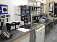
Here's pictures I found of a different unit in a chip foundry somewhere... three different views of the process console and the last is the solution console (dispensing unit).
Incidentally, one of the parts I have for this system was accompanied by a requisition form from within National Semiconductor, and I know International Rectifier and IBM have or had these as well.
This is the controller for the FSI 'Saturn' wafer processor system. (which makes part of cj7hawk's post ironic)
I used to work on the various boards in this system and recently got a wild hair to get this system documented as to all the circuit boards etc.
I even found an already scanned copy of the operator's manual and a physical copy the tech book (blueprints etc. of all the major components) which I did scan as well.
I wish I knew what kind of paper the tech book pages were printed on as it does NOT tear. It almost feels like a cross between regular paper and Tyvek.
Once I'm reasonably sure I have all the boards documented (I have one of the 'flow control' units - the ones with the chemical names on them - enroute), I'll see about making each board has unique part identifiers.
I ran into that when trying to make the overall system schematic hierarchical.
Here's pictures I found of a different unit in a chip foundry somewhere... three different views of the process console and the last is the solution console (dispensing unit).
Incidentally, one of the parts I have for this system was accompanied by a requisition form from within National Semiconductor, and I know International Rectifier and IBM have or had these as well.
Attachments
cj7hawk
Veteran Member
Are you making your own chips? Or just fixing someone else's equipment?
Sounds like a cool project
Sounds like a cool project
tech58761
Experienced Member
Thanks!
I just remember working on the various components and we had a shelf and two benches full of testers for all these subassemblies, and I got to wondering if and how all these parts worked together.
One of the prints I scanned which shows the system side:
I just remember working on the various components and we had a shelf and two benches full of testers for all these subassemblies, and I got to wondering if and how all these parts worked together.
One of the prints I scanned which shows the system side:
Attachments
segaloco
Experienced Member
- Joined
- Apr 30, 2023
- Messages
- 338
Neat, yeah HF in particular gives me the willies, it was part of a cleaning solution I used once upon a time for cleaning inductively coupled plasma torches. I don't know enough about good schematic design to offer effective critique but I appreciate the cleanness of what you've shared.
tech58761
Experienced Member
Yeah, I wouldn't want to come near HF either... you can't even keep it in a glass bottle!
Thank you for the feedback - it's good to know I'm on the right track in general.
Thank you for the feedback - it's good to know I'm on the right track in general.
tech58761
Experienced Member
I've also begun working on an overall description of the unit and a board by board description.
I'll also be getting my grimy paws on the last of the assemblies that are still easy to find (the latest status is it's been in the Twin Cities since the crack of Monday).
I'll also be getting my grimy paws on the last of the assemblies that are still easy to find (the latest status is it's been in the Twin Cities since the crack of Monday).
cj7hawk
Veteran Member
I've also begun working on an overall description of the unit and a board by board description. I'll also be getting my grimy paws on the last of the assemblies that are still easy to find.
I sometimes wonder how easy it would be to rebuild the world and recover even this kind of technology if there was a severe enough war or cataclysmic event that caused most current knowledge to be lost... We all live right at the top of a technological house of cards right now

tech58761
Experienced Member
Bitterly cold up here in the northern plains... have to wait one more day for delivery. I did find some information that suggests that various key parts (particularly the 8085, 8031, and 8155) going EOL in the late '90s may have led to that system's discontinuance. The next generation system used a rack-mounted DOS PC based on the STD Bus arrangement as its controller.
Hugo Holden
Veteran Member
Just wanted to see what others think of these schematic diagrams I've sketched...
I'm not trying to be a buzz killer here, or be insulting or over critical. I'm just trying to say what I think is the better way to draw schematics.
Ideally the schematic flows from left to right, as though your were reading it. The devices are better configured to show what is going on inside them.
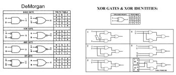
With logic circuits, especially logic gates, all gates should be drawn as their DeMorgan equivalents. In other words, lets say you have a two input gate where there is a high output, where both lines have to be low to achieve it together, you don't draw it as a NOR gate, but instead in its negative logic form as an AND gate with inverted inputs.
The whole idea of a good schematic, is to help a person looking at it understand what the circuit is trying to do. This is because, mostly people consult a schematic when the thing is broken and they are trying to fix it.
To fix something, most of the time, you have to figure out its design and why it works in the first place.
Unfortunately, there is a tendency of some schematic software to draw all the IC's as black boxes with multiple interconnects, even though they do a good job of labeling the pins on them, often to create Netlist to make pcb's, but this sort of diagram looks more like a Refrigeration Engineer from the year 1940 created it, and is mostly useless for understanding how it works and for fault finding.
A properly drawn schematic may well be becoming increasingly rare.For example it should be federal crime to draw a 74LS245 as a black rectangle. The idea is to minimize the time the service engineer has to go hunting out data sheets.
In summary I think the schematics you created are not ideal, and only of use to create a pcb, and of very little use in conveying how the circuitry works or helping to fault find it, but again this remark is not meant to be harsh and just an opinion from a person who has studied all sorts of schematics from the 1920's to current times.
Last edited:
cj7hawk
Veteran Member
I'm not trying to be a buzz killer here, or be insulting or over critical. I'm just trying to say what I think is the better way to draw schematics.
Ideally the schematic flows from left to right, as though your were reading it. The devices are better configured to show what is going on inside them.
With logic circuits, especially logic gates, all gates should be drawn as their DeMorgan equivalents. In other words, lets say you have a two input gate where there is a high output, where both lines have to be low to achieve it together, you don't draw it as a NOR gate, but instead in its negative logic form as an AND gate with inverted inputs.
The whole idea of a good schematic, is to help a person looking at it understand what the circuit is trying to do. This is because, mostly people consult a schematic when the thing is broken and they are trying to fix it.
To fix something, most of the time, you have to figure out its design and why it works in the first place.
Unfortunately, there is a tendency of some schematic software to draw all the IC's as black boxes with multiple interconnects, even though they do a good job of labeling the pins on them, often to create Netlist to make pcb's, but this sort of diagram looks more like a Refrigeration Engineer from the year 1940 created it, and is mostly useless for understanding how it works and for fault finding.
A properly drawn schematic may well be becoming increasingly rare.For example it should be federal crime to draw a 74LS245 as a black rectangle. The idea is to minimize the time the service engineer has to go hunting out data sheets.
In summary I think the schematics you created are not ideal, and only of use to create a pcb, and of very little use in conveying how the circuitry works or helping to fault find it, but again this remark is not meant to be harsh and just an opinion from a person who has studied all sorts of schematics from the 1920's to current times.
Can you offer an exemplar to view? I'm quite curious - I've never heard of DeMorgan equivalents before.
tech58761
Experienced Member
Why use the DeMorgan equivalent by default? I do have one other schematic drawn for another product where it did make sense to use the DeMorgan equivalent on one gate...
I do plan to go back through all the custom symbols I've made soon and update them to show inversion on the inputs where needed.
cj7hawk: For example, the DeMorgan equivalent of a NOR gate is an AND gate with the equivalent of inverters on the input. (implementation of DeMorgan's Theorem)
I do plan to go back through all the custom symbols I've made soon and update them to show inversion on the inputs where needed.
cj7hawk: For example, the DeMorgan equivalent of a NOR gate is an AND gate with the equivalent of inverters on the input. (implementation of DeMorgan's Theorem)
tech58761
Experienced Member
Hugo: Up to now, my goal was just to get everything down on paper. Now that I have 99% of the data I was after, I am actually going back and trying to regroup the schematics so they flow better.
Hugo Holden
Veteran Member
You don't use the DeMorgan equivalent by default. You switch to the DeMorgan equivalent to help the person reading the schematic understand what the circuit is doing.Why use the DeMorgan equivalent by default? I do have one other schematic drawn for another product where it did make sense to use the DeMorgan equivalent on one gate...
I do plan to go back through all the custom symbols I've made soon and update them to show inversion on the inputs where needed.
cj7hawk: For example, the DeMorgan equivalent of a NOR gate is an AND gate with the equivalent of inverters on the input. (implementation of DeMorgan's Theorem)
For example if you have a two input gate where the use of it is that its output goes low when both of its inputs are high at the same time, of course you draw it as a NAND gate.
However if you had the same NAND gate in another circuit, where its output went high, if either of its input signals went low, it should be drawn as an OR gate with inverted inputs. In both cases the actual device is still a NAND gate, but drawn in the NAND gate form or the DeMorgan equivalent, is done depending on how the circuit design is operating.
Often you will see schematics with many NAND gates (and not a sign of an inverted input OR gate), and the person who made the published schematic, probably was making the pcb file, and doesn't understand the circuit's operating theory. They just created the "connection diagram" by linking pin numbers on IC packages. While it might be correct, it is not helpful for servicing. Once you figure the circuit's logic out, some are being used as DeMorgan equivalent inverted input OR gates, so it is always better that the designer makes the schematic and puts in the DeMorgan equivalents, where they are required, or it leaves a service technician further in the dark about what is happening in the logic.
If you look the DeMorgan theory up, you will also find that a NOR gate can be drawn as a negated input AND gate and in some particular circuit, it may be being used in that manner and therefore it should drawn in that manner on the schematic.
Knowledge of the DeMorgan theorem also helps when designing circuits, lets say you want to make some sort of decoder circuit looking at up to 8 data bits and you want to detect when all 8 bits are zero at the same time, and you want a high output, or a ZERO signal, then DeMorgan tells you to reach for an 8 input NOR gate. But if you draw that in your schematic as a NOR gate, it won't do a technician any favors.
I have attached a useful data sheet.
Also there is another thing, the XOR gate. There are a number of circuit configurations that behave as XOR, and it can be very confusing to figure out if the designer does not explain when these are used, aside from using an actual single XOR gate, the sub-circuit should have a box around it. One of the more interesting versions of the equivalent of XOR was discovered in Atari's arcade Pong circuit from 1972. One really odd thing was that there was a spare single XOR gate in a package nearby that was not used, but the designer chose to make it in a very creative manner instead. When I asked him why he didn't just use the XOR gate nearby, he was not sure. When the circuit was published, there was no technical description of how it worked, not in any detail at least, and that part of the circuit certainly had many baffled.
Attachments
Last edited:
tech58761
Experienced Member
My main goal at this point was building a netlist for each of the boards I'd acquired over the last few months and transcribing them into KiCAD. My next step was that once I got a better sense of what's going on, then I was going to start rearranging / redrawing these schematics accordingly. The more I look at some of these drawings now, the less confident I become that I was on the right track. When I make my own IC symbols, again, I at least sought out the datasheets and tried to make a logical arrangement of the pins (Ultra Librarian sucks - their so-called symbols are nothing but script-generated 'black boxes'), and I wasn't above moving pins around if it helps make the schematic arrange better. Most of these other schematics consist mainly of inverting buffers, Schmitt triggers, or 'boxes' dealing with buses or higher-level functions; it was only a literal handful (like the CPU and Comm boards) that include glue logic gates. Now that I have acquired, transcribed, and dumped (as needed) all the boards for this system that I can reasonably hope to acquire, I'm almost tempted to just move everything aside and refocus on other projects that need my attention...
tech58761
Experienced Member
So, many of my diagrams for these boards were already arranged as you say, and a few like the Communications and Display boards were relatively easy to rearrange.
The I/F and I/O boards were a challenge to fit on one sheet, and rearranging them is a bit daunting, as parts of both are bidirectional... and so is the system interface that both boards connect to.
The thought of starting over, just... no. Bottled up and set aside for a while.
The I/F and I/O boards were a challenge to fit on one sheet, and rearranging them is a bit daunting, as parts of both are bidirectional... and so is the system interface that both boards connect to.
The thought of starting over, just... no. Bottled up and set aside for a while.
tech58761
Experienced Member
cj7hawk
Veteran Member
They flow nicely.
I don't have any idea of whats on the board from a physical perspective, but I can get an idea of the functional structure of the PCB from those. Do the references on the schematic reflect the locations of the chips on the actual PCB?
I don't have any idea of whats on the board from a physical perspective, but I can get an idea of the functional structure of the PCB from those. Do the references on the schematic reflect the locations of the chips on the actual PCB?