Upcoming Events:
- VCF South West - June 14 - 16, Davidson-Gundy Alumni Center at University of Texas at Dallas
- VCF West - Aug 2 - 3, Computer History Museum, Mountain View, CA
- VCF Midwest - Sept 7 - 8 2024, Schaumburg, IL
- VCF SoCal - Mid February 2025, Location TBD, Southern CA
- VCF East - April 2025, Infoage Museum, Wall NJ
-
Please review our updated Terms and Rules here
You are using an out of date browser. It may not display this or other websites correctly.
You should upgrade or use an alternative browser.
You should upgrade or use an alternative browser.
Setting up a DECnet network with a Pro380 and Windows client?
- Thread starter stanp
- Start date
I found XACKAL connects to the input enable on two 373 latches and pin 13 on a 74LS00 (input to a NAND gate) on the other side of the board - likely part of the bus reply generator in the figure above.So XACKAL is also connected to the BRPLYL circuit, not just the latch. I don't think you need to trace it.
I have an unexpected result and I am not sure what to make of it. I patched together a program to enumerate the CTI cards, read the card ID, find the DECNA card and then perform the exact memory test from the diagnostic ROM. The card enumeration and ID code is based on davibear's code. As a starting test, I just enumerated the cards and their IDs. I have three cards in the cage: Slot 1: HDD controller (401), Slot 2: Floppy controller (2004), and Slot 3: DECNA card (42). The program runs and reports the following:
Slot 1: ID 401
Slot 2: ID 2004
Slot 3: ID 424 (not 42)
I moved the DECNA card to slot 6 with the same result. I'm looking for a bug in the code, but not finding one. It reports properly for the HDD and Floppy controllers. The PRO diagnostic does report ID 42 in the start-up error. I asked how could that be if I am reading 424? The ROM disassembly shows an immediate value of 42 is stuffed into a register for the return instead of reading the ID from the top of the ROM. The maintenance disk does recognize the card as DECNA. Could my ROM possibly have 424 as the ID? Or is this a symptom of a card failure with the data lines? I'm happy to post the code if anyone wants to take a look. I haven't run the memory test. Maybe I can accept the 424 and continue?
One possibility is the that control register has the bit set to the Address ROM, even though the control register reset state of 0 should point to the Option ROM. I could try first clearing the control register for that slot. According to the tech manual, "The first six bytes [of the Address ROM] contain the unique address and are accessible via the ROM data window register. The next two bytes contain a checksum value for PROM contents and are also accessible through the ROM data window register." The 424 doesn't seem match the address info on the card.
Is the following correct for the DECNA card? I cannot find mention of the offsets in the tech manuals:
ROM Data Register Base + 0
ROM Address Counter Base + 2
ROM Control Register Base + 4
ROM Memory Base Address Register Base + 6
Last edited:
MattisLind
Veteran Member
Are you certain that the ROM address counter is reset when reading the ROM Data register? I.e have you written to the ROM address register in order to reset the counter?I have an unexpected result and I am not sure what to make of it. I patched together a program to enumerate the CTI cards, read the card ID, find the DECNA card and then perform the exact memory test from the diagnostic ROM. The card enumeration and ID code is based on davibear's code. As a starting test, I just enumerated the cards and their IDs. I have three cards in the cage: Slot 1: HDD controller (401), Slot 2: Floppy controller (2004), and Slot 3: DECNA card (42). The program runs and reports the following:
Slot 1: ID 401
Slot 2: ID 2004
Slot 3: ID 424 (not 42)
I moved the DECNA card to slot 6 with the same result. I'm looking for a bug in the code, but not finding one. It reports properly for the HDD and Floppy controllers. The PRO diagnostic does report ID 42 in the start-up error. I asked how could that be if I am reading 424? The ROM disassembly shows an immediate value of 42 is stuffed into a register for the return instead of reading the ID from the top of the ROM. The maintenance disk does recognize the card as DECNA. Could my ROM possibly have 424 as the ID? Or is this a symptom of a card failure with the data lines? I'm happy to post the code if anyone wants to take a look. I haven't run the memory test. Maybe I can accept the 424 and continue?
One possibility is the that control register has the bit set to the Address ROM, even though the control register reset state of 0 should point to the Option ROM. I could try first clearing the control register for that slot. According to the tech manual, "The first six bytes [of the Address ROM] contain the unique address and are accessible via the ROM data window register. The next two bytes contain a checksum value for PROM contents and are also accessible through the ROM data window register." The 424 doesn't seem match the address info on the card.
Is the following correct for the DECNA card? I cannot find mention of the offsets in the tech manuals:
ROM Data Register Base + 0
ROM Address Counter Base + 2
ROM Control Register Base + 4
ROM Memory Base Address Register Base + 6
I don't think the HDD nor the floppy controller had a Diag ROM as the DECNA has. They only have one single word that is the ID.
The register layout is correct as far as I see. Unfortunately the tech manual is rather bad. It lacks a lot of interesting details.
I stuck a memory card in the cage to test MattisLind's suggestion. The memory card is octal 34. The result came back as 344. So, it is definitely a bug. I'll bet it has something to do with the QIOW string.
Bingo! I replaced the length calculation in the QIOW$S call with the returned length from the $EDMSG macro and that fixed the problem. The hint was the "4" and the preceding reporting of "2004" that extended the string by one byte.
Bingo! I replaced the length calculation in the QIOW$S call with the returned length from the $EDMSG macro and that fixed the problem. The hint was the "4" and the preceding reporting of "2004" that extended the string by one byte.
Last edited:
Here's an update on my DECNA card debug. My program to test DECNA card memory led me on an educational journey to learn things that some of you probably know. After fixing the length calculation in the QIOW$S call, I proceeded to debug the memory test portion. It seemed to run, but I needed a way to determine if I was actually hitting the DECNA card with reads and writes. I tried different techniques including removing the card, but eventually found that turning off memory access in the 8207 to trigger a Trap 4 event with a bus reply timeout was best once I had confidence in the code to write the control register. I assembled, linked and ran the program from the P/OS Toolkit. I linked the program with /PR as a privileged task. I discovered that when you link it this way, it places the program in APR 5 space by default and you can choose APR 0, 4 or 5. The program does not run in kernel mode, but user mode. For that reason, my attempts to program kernel PARs yielded no results. Upon realizing this, I attempted to run in kernel mode by changing the PSW. But the mode bits are protected and trigger a Trap 4. I tried to install an error handler, but that froze the machine (maybe halted it). I then discovered the $SWSTK call for this purpose, but then determined it does not exist in P/OS. However, SWST$ exists and allows one to run a subroutine in kernel mode and return back to User mode rather than switch to kernel mode. A small test program showed SWST$ worked, but running in kernel mode for the memory check is probably not best. So, I returned to user space and found my changes to User PAR were not having their desired effect. I set tried both instruction and data space and later confirmed I was running in a mode that only the instruction space PARs are used. I also found I could not change User PAR 5, presumably because it is used by the code when linked with privilege. But I could alter User PAR 6 and User PAR 4. However, my debug code using QIOW$S was unknowingly causing unexpected problems. I discovered after much debug that even though I set PAR4 and called QIOW$S and $EDMSG to print the value to the terminal, my PAR 4 was being overwritten by the macro calls. So, while the screen message showed the right PAR, it was getting after the print. If I read the PAR and printed it consecutively, the change in PAR value from my value of 144000 to 1000 became evident. My takeaway is that if you set a PAR directly, don't assume it is still in place after calling a system macro. In fact, I think the technique of directly setting PARs is probably not good. There are macros such as CRAW$ and WDBBK$ to create virtual address windows and set the PARs. I haven't tried them yet under P/OS, but I suspect it may address the unexpected reset of the PARs. I tried this approach under RT-11 with success previously.
Getting past this problem and satisfying myself that the code was actually hitting the DECNA card by turning memory access on and off and triggering Trap 4 when off, my memory tests immediately showed a problem. I tried to write 0x0, 0xAAAA (125252) and 0x5555 (52525) and read back the results. I started with the lower block of 64KB and got the following:
0x0000 --> 060136
0xAAAA (125252) -> 165336
0x5555 (52525) -> 072537
The good news is that some bits are actually responding, so I am confident that I am hitting the card. If you break it down by bit you find errors as follows:
15 14 13 12 11 10 9 8 7 6 5 4 3 2 1 0
G B B G G G G G G B B B B B B G G= good, B= Bad
This helps me identify which memory chips in the two columns of memory on the board may be bad, assuming I can determine whether the top of the column is bit 15 or bit 0. However, I then decided to check the upper 64KB of memory in the next row. I found the same result. I am thinking now the issue may not be the memory but instead a common buffer or latch, unless bad memory chips are forcing various bits of the data bus high or low. Any thoughts on whether this is a memory chip or buffer/latch problem and method to test which is at fault? It could be a data-in problem or a data-out problem. I assume the 8207 is working properly since I can map the memory, turn it on and off. and get some bits through.
Some have asked for the updated maintenance disk. I will post once I get a chance to clean up.
MattisLind
Veteran Member
The lower and upper 64k are the same chips. The memory array is 64kx16. IMHO having this many DRAM-chips going bad is not very likely.
You could test the theory by removing one of the chip that always reads 0 and re-run the test.
Could there be a bad buffer? I am mostly thinking that bad buffers affect the bus in the same way for all bits. Either stuck high or stuck low. In this case it seems that both things happens.
It could be a bad buffer, which has failed partially. Or both buffer chips that failed partially, depending on how DEC decided to route the bus. It can be a combination of bad RAM chips and bad buffer.
Perhaps you can pull out the board and power it from a lab power supply and measure the signal level on the data bits on the inputs and outputs the memory? Strange levels may reveal bad chips.
When I am thinking of it, we are not sure if it is the data written that is bad or the data read since data goes through a buffer when writing and is latched when read back.
Thanks. I pulled the board and realized exactly what you said. In fixing and running the ROM code over my simple memory test, I found there are some locations where one of the bits toggles to the correct value. I located the 244 buffers and 373 D latches. Like you said, it could be an input or output problem. I could potentially power the board on the bench. Is it just a single 5V supply?
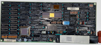
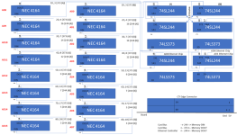
Success! After considering some possible options, I decided that it was unlikely the LS logic had gone bad even though there were potentially 8 bad memory chips. Those transceiver and D latches are practically indestructible in my experience. I instead decided to trace the board to identify which chips in the two columns of memory were associated with the bad bits. I made the attached diagram of the memory, buffers and latches. The Rosetta stone was the Ethernet controller, where I could trace a labelled address/data line to a memory chip. It turns out the outer memory column is D8 to D15 (top to bottom) and the inner column is D0 to D7 (top to bottom). I then desoldered and replaced one memory chip to confirm the expected bit was responsive. To avoid desoldering in the future, I inserted chip sockets hoping that would not alter the bus characteristics. With all 8 chips replaced, the card passed the boot-up check and successfully passed the maintenance disk check.
It also passed by memory program check. But as I started to expand my memory check beyond the first 512 words, I encountered problems with the PARs unrelated to the hardware and I really started to question how to properly write a macro 11 program to reach memory at a specific physical location. All my testing suggests that if the program directly changes PAR values without informing the OS, any change in task, for instance, caused by an interrupt or system call, risks the OS restoring the PARs to the values it knows, leaving your program reaching the wrong memory space when back in context. For instance, I started writing my program in the following manner:
Reset and program memory register on DECNET card
Set PAR and PDR values
Set base virtual address corresponding to the APR
Set loop counter
Write memory
Read memory and increment base virtual address
Compare read and write values, branch on mismatch
Decrement counter and loop to write next memory address
I found this works when the loop counter was about 1000 (512.) or less. When I tried 3000, it triggered a trap with the register set display showing it aborted about 1700. No matter which APR I tried, I could not get past this value to reach the remainder of the virtual address window and the value itself was not constant, but near 1700. I had previously confirmed that a call to system macro would change my PAR. I then rewrote my loop to disable interrupts, figuring an ISR or the restoration was changing my PAR. Although I could get away with a 1000 loop, anything longer would get caught in an interrupt. The code then became:
Reset and program memory register on DECNET card
Set base virtual address corresponding to the APR
Set loop counter
Disable interrupts
Set PAR and PDR values
Write memory
Read memory and increment base virtual address
Re-enable interrupts
Compare read and write values, branch on mismatch
Decrement counter and loop to set PAR/PDR again and write next memory address
This worked and I was able to loop through the full 8KB of virtual address space. But in disabling all interrupts, including the clock, I lost my blinking cursor. The system remained stable, but doubts linger about possibly overwriting memory. If I disabled/enabled interrupts, but did not include setting the PAR/PDR in the loop, it would trap again. One thing that seems to be clear is that if you don't inform the OS/memory management unit that you are reserving a PAR, it is going to restore it to the value it understands to be correct upon any task change. We encountered something similar in another VCF thread on PRO video with RT-11. Again, we are disabling and enabling interrupts with direct PAR access. Nowhere in the macro programming training manuals do they discuss directly setting PARs. They instead describe a group of CRAW, CRRG, and other macros to formally request a memory block, create a region, create a virtual window, and map the window to the region through an APR. But these macros let the memory management unit select the physical memory and of course set the PAR. But we want to specify a specific region of physical memory. How do you inform the OS/memory management unit that you want to assign a specific part of physical memory to a region and window so that it will set the proper PAR and not mess with it when interrupts and other things occur? The POS Driver manual talks about a $STPAR call to add option card memory to the system and how to install a driver into the system, but I haven't found a way to specify a block of physical memory without directly setting a PAR. Should I be running in kernel/system mode? Would that let my PARs stick?


Last edited:
I was going to change all memory, but every rework operation poses some risk to the board. So, I decided to just change out what was necessary at this point. If others go bad, I can replace and socket. Now that the card is functional, I need to return to setting up a network with a PC running PathWorks. But this issue with the PARs is really bugging me. I encountered it now twice in two different projects with no good approach.Nicely done. Good move to just replace all the chips, if one goes bad the rest are probably on the way. So have you got DECNET up and running again?
MattisLind
Veteran Member
Good job! 8 bad chips out of 16 is really not what I expected.
Can you please check one more thing on the board before you put it back in the machine permanently? Is pin 17 on the Fujitsu MB502 (24 pin CER-DIP) tied to ground or pullup / Vcc?
Can you please check one more thing on the board before you put it back in the machine permanently? Is pin 17 on the Fujitsu MB502 (24 pin CER-DIP) tied to ground or pullup / Vcc?
Pin 17 is pulled up to VCC.Good job! 8 bad chips out of 16 is really not what I expected.
Can you please check one more thing on the board before you put it back in the machine permanently? Is pin 17 on the Fujitsu MB502 (24 pin CER-DIP) tied to ground or pullup / Vcc?

