saipan59
Experienced Member
Hi Mark, attached are schematics.
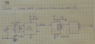
One shows the time base used on the clock. Datasheets are on the web.
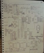
The other is for the T11 wire-wrap board. It's quite a mess...
The stuff in the lower-left corner (HC595's) was never implemented. It was a plan to make an interface that would be driven by a modern MPU, to DMA code into the RAM for the T11. I was going to use an MSP430. Every time on power-up, the MSP430 would load the T11's RAM and let it run. So, the T11 wouldn't need any EEPROM. The HC595's were a serial-to-parallel interface, so that only a few wires would be needed coming from the MSP430.
I've had thoughts of something similar with a uVAX-II board pair in a Qbus backplane for power: On power-up, an MPU would write code into RAM via the console ODT, then run it. But, it's only practical for smaller programs, and I can't think of what I would do with it...
One of the HP LED displays is shown in the lower-right corner, connected to the LS138. Those particular displays are sorta expensive today. I've got a few extra, but I'm not sharing .
.
The LS374 on the right side was not implemented. It was for adding output bits, but the clock doesn't need it.
The LS240 in the upper-left corner has two sections - one is for the T11 power-up config bits, the other is 4 bits of Input, selected by the "BTN" signal, which is addressed at the upper-most 1K page of the "B6" 8K page. Two bits are for the buttons, one is for the 3 Hz input (not shown on the drawing, I think it's pin 8 of the LS240), the 4th is unused.
The notations next to most chips pins, such as "3-24", are the row/column for the physical pin on the wire-wrap board I used.
Pete


One shows the time base used on the clock. Datasheets are on the web.
The other is for the T11 wire-wrap board. It's quite a mess...
The stuff in the lower-left corner (HC595's) was never implemented. It was a plan to make an interface that would be driven by a modern MPU, to DMA code into the RAM for the T11. I was going to use an MSP430. Every time on power-up, the MSP430 would load the T11's RAM and let it run. So, the T11 wouldn't need any EEPROM. The HC595's were a serial-to-parallel interface, so that only a few wires would be needed coming from the MSP430.
I've had thoughts of something similar with a uVAX-II board pair in a Qbus backplane for power: On power-up, an MPU would write code into RAM via the console ODT, then run it. But, it's only practical for smaller programs, and I can't think of what I would do with it...
One of the HP LED displays is shown in the lower-right corner, connected to the LS138. Those particular displays are sorta expensive today. I've got a few extra, but I'm not sharing
The LS374 on the right side was not implemented. It was for adding output bits, but the clock doesn't need it.
The LS240 in the upper-left corner has two sections - one is for the T11 power-up config bits, the other is 4 bits of Input, selected by the "BTN" signal, which is addressed at the upper-most 1K page of the "B6" 8K page. Two bits are for the buttons, one is for the 3 Hz input (not shown on the drawing, I think it's pin 8 of the LS240), the 4th is unused.
The notations next to most chips pins, such as "3-24", are the row/column for the physical pin on the wire-wrap board I used.
Pete
