• Please review our updated Terms and Rules here

Theory of operation of H7441 regulator

thunter0512

Veteran Member
Joined
Sep 27, 2020
Messages
859
Location
Perth in Western Australia
The DEC H7441 regulator is a relatively complex circuit using two 555 timers and two LM301 op-amps.
I am struggling to understand how it is meant to work and was hoping to find a maintenance manual for it.
Could anyone with such a manual please help?

Alternatively is there another explanation of the operation of this or similar types of circuits?
 
Thanks for the replies, but neither of them addressed my question about the theory of operation or the detailed operating principle of the circuit.

The circuit implements a switch mode supply.
One of the two 555 timers operates as a oscillator, the second I think operates as a monoflop with the pulse length controlled via one of the LM301s.
Overall the circuit seems very complex and while I understand parts of it, other parts are mysterious.

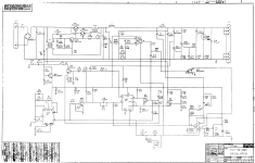
Here are the schematics (click on the image to see it full size):

H7441.png

I am hoping there is some contemporary document describing this (for me) unusual and complex implementation, or similar ones (2 x 555, 2 x LM301, 2 x transformers, 2 x inductors).

In particular the top left section around Q1/Q2/Q3 and T1/T2 and E3 is most confusing.

I did not find anything remotely similar in "The Art of Electronics" from Horowitz & Winfield.
 
Brent Hilpert over at cctalk was so kind to provide a beautiful description of the H7441 circuit. I thought it might benefit others in the future to have this information available in this forum, so I have copied Brent's description below:

The basic form is that of a switching inductive buck/step-down regulator.

L1 is the main bucking inductor.
D12 is the inductor discharge diode for the bucking operation.
Q1 and Q2 are the main switching transistors, operating in parallel with T2 in their emitter circuits to balance current through the two transistors.
Q3 is a driver stage for Q1,Q2.
C11,L2,C16 are the main output filter.

Fixed-frequency oscillator E1 triggers variable-width monostable E2 via Q6 to create the PWM switching pulses.
Q8 and associated form a constant-current source for the timing capacitor C10 of this PWM-monostable, to linearize the charge curve of the capacitor for better operation of the pulse-width timing.

The switching pulses from the PWM-mono are amplified by Q5 to drive T1.
T1 provides galvanic (voltage) isolation to shift the pulses up to the higher operating voltage of Q1,Q2,Q3.
All base-drive energy for Q1 and Q2 is delivered through Q3 from T1, thus Q5 driving T1 must itself be a reasonably hefty driver.
Excessive current through Q5 produces a V-drop across R10 which may turn on Q7 to take the PWM-mono into reset (E2.4=low).
D7,D8,R7 clamp and sink reverse voltage/energy from the T1 secondary to avoid reverse breakdown/damage to Q1,Q2,Q3.

Op-amp E4 is the voltage-sense amplifier for the main regulation feedback loop.
D18 and associated provide the master reference voltage.
An increase in the sensed +5 output voltage presented at -input E4.2 relative to the reference voltage at +input E4.3 lowers the voltage into the PWM-mono control input E2.5 to shorten the ON-width of the switching pulses, and vice-versa for a decrease in the +5 output.

Op-amp E3 is running open-loop to function as a comparator for over-current sense.
R17,R18 are the current-sense resistors, placed here in the negative supply line of the +5 main output.
If the current-induced voltage drop across R17,R18 becomes high enough, E3 trips high, turning on Q7 to take the PWM-mono into reset.
R19,R20 provide the counter-bias V that the R17,R18 V-drop must overcome to trip E3.
E3 tripping high also turns on Q9 to short the reference voltage to GND at E4.3, to minimize the ON-width of the switching pulses.

D20,D21,D22 form a crowbar for the +5 output.
The crowbar tripping performs two actions: shorting the +5 output via D19, as well as shorting the switching pulses at the base of Q5 via D23 so the supply doesn't keep pumping energy into the shorted output.

D2,Q4 and associated form a simple linear regulator for internal supply of ~ +12V to the control electronics.
C7,D17,D25,C8 are a little charge pump driven off oscillator E1 to create a negative V supply for the op-amps E3,E4.


Thanks to Brent Hilpert!
 
I see that someone has already provided an explanation, but you may also find some items of interest in the following DEC document beginning on page 3-10:

DEC-11-HBKEF-A-D BA11-K Mounting Box Manual
Sorry but hat manual on page 3-10 describes a H744 which is entirely different from the H7441 which is the subject of this topic and as described by Brent in his cctalk message which I quoted above. The only similarity in the two supplies is that both provide +5V.
 
I will have to go through in detail, but at a glance, this is what I am seeing:

- D1/F1/C1 provide fused rectified unregulated DC (voltage depends on what is hooked to J1).
- Q4 provides an unregulated 12V to power the rest of the regulator

-E1, as you said, is an oscillator providing a pulse train to the rest of the circuit, used for PWM and a negative voltage reference.

-D17, D25, C5 provide a negative voltage rail for the LM301's

- E2 is a PWM circuit, diiscussed in pieces below:

- The output pin 3 drives the primary of T1, producing current on the secondary, which is rectified to activate Q3.

- Q1 and Q2 are parallel power transistors acting as a single NPN transistor the differential choke provides a reactive ballast, canceling the small differences due to mismatch without the constant loss of ballast resistors.

- Q3 and Q1+Q2 form a Sziklai pair pass element, driving L1 + L2, which form the output inductor and C16 stores the passed charge, smoothing the output voltage.

- D20 and D21 implement overvoltage protection. D20 crowbars the output to ground, and D21 inhibits the PWM output of E2.

- Here's how I think the PWM works, with some simplifications. The timing of the various events below will be voltage dependent, and depending on charge rates, some steps could be flipped.
  • LM301 E4 provides a negative feedback signal with DC offset, applied to the E3 pin 5 Control Input, and to C6 at the Trigger input (E3 pin 2)
  • With E1 pin 3 output low, Q6 is off, and the Trigger rests at the offset error level.
  • When E1 pin 3 output goes high, Q6 is on, and the low side of C6 is pulled close to ground, activating the trigger of E2, bringing E2 output pin 3 high, turning off the DISCHARGE trnasistor.
  • Once DISCHARGE is off, Q8,R23, D14, D15, R24 form a current source that charges C10 until the voltage matches the feedback output of E4, at which point E2 output resets and C10 is discharged. Larger error signals mean lower control voltage, and quicker threshold, so shorter PWM pulses.

- The LM301 E3 is a comparator sensing the return current. An overcurrent forces the output high, holding the E2 (PWM) 555 timer in the RESET state via Q7, and grounding the reference voltage to the E4 error amplifier via Q9, minimizing the pulse width.

- There are a few other variables such as the CTL signal also charges C6, so the triggered state is released sooner for low output voltages and later for high output voltages. This could also stretch or shrink the duty cycle, depending on relative charge rates of C10 and C6. Or this could not kick in until E3 grounds the postive input of E4, which could then potentially delay the release of the trigger long enough to completely inhibit the pulse. A scope would be helpful.
 
Last edited:
Shoot, somebody posted a description already! I had this in draft since last night, and just did some edits and posted. At a glance the breakdown seems to be similar.
 
Shoot, somebody posted a description already! I had this in draft since last night, and just did some edits and posted. At a glance the breakdown seems to be similar.
Thank you for taking the time to prepare, organize, edit, and post your analysis. I appreciate both perspectives. My cup runneth over :-}!

This is one of those areas where the lack of extant DEC documentation beyond the FMPS leaves us in a tough spot. No longer!
 
I will have to go through in detail, but at a glance, this is what I am seeing:
...

Thank you very much Dfnr2 for your time and effort to describe this for me somewhat obscure circuit.
I understood parts of it, but you (and Brent) have nicely described details I didn't grasp before I asked for help.

I am sure others will struggle with the H7441 in the future, so this topic should help.
 
  • Once DISCHARGE is off, Q8,R23, D14, D15, R24 form a current source that charges C10 until the voltage matches the feedback output of E4, at which point E2 output resets and C10 is discharged. Larger error signals mean lower control voltage, and quicker threshold, so shorter PWM pulses.
Just to clarify: By "Larger error signals" I meant larger overvoltage error. Undervoltage will generate larger feedback voltage and stretch the pulses.
 
Back
Top