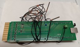
VCF straight 8 was intermittently acting up again. Tried the board wiggle test and seemed to be sensitive around the R211 MA, MB, PC registers. There are 12 of those cards. Couldn't localize to one card. Tried my contact resistance checking card. I made this when originally restoring the machine to try to deal with intermittent connections on the cards. It shows current, minimum and maximum contact resistance when ssh'd into from my laptop. Did show some of the contacts which varied by slot had high resistance. Good contacts you could wiggle the board in slot and resistance stayed below an ohm. Bad contacts showed maximum resistance it could display of 8 ohms. Either when just inserted or when wiggled. Was able to get resistance down with various cleaning methods but some still changed with wiggling card. Tried to check contact force by probing contacts by hand. Inconclusive. Will need to bring a gauge to check contact force and investigate further if I can reproduce on spare backplane here.
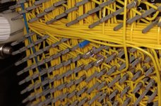
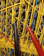
And got the expected result after going through all the effort of no change in symptoms. Tried brushing hand over wirewrap pins on those cards and it triggered incorrect operation. Sometimes one of the memory address register bits didn't seem to load with examine switch. Inspecting that pin I could see a bad solder joint where they had used a bus strip to connect pins across all the R211 cards. See pin where the red clip is on. That is pin PC16-M which is PC->MA (Transfer program counter to memory address register). You set the PC to address you want to read with load address then examine switch transfer it to MA register to read memory and increments PC.
Didn't think I could resolder without damage to wires to added a purple wirewrap to the next pin. Could then wiggle cards and pins without crashing the moving light demo.
Next was working on the A/D converter. It looked like the machine originally didn't have that option installed. Likely the The R.E.S.I.S.T.O.R.S. got the cards and installed them but it wasn't in a working state. The manual said you just had to install the cards but it looked like you had to also remove some wires to enable it. VCF management agreed that it was ok to remove the wires to enable the A/D converter.
I started troubleshooting the converter. First issue was the R401 card in PE13 wasn't generating the conversion clock. I replaced a bad diode on the card to fix. Most of the logic in the PDP-8 is done with discrete diodes.
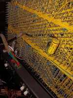
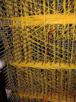
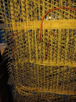
Next issue was the memory buffer register wasn't shifting. The shift signal from the A/D converter was grounded to prevent noise pickup when the A/D wasn't installed. They used red to mark the wires that needed to be removed to install options. Not sure what orange and green wires signify. I removed the wire from MB SHIFT (pin DU). Also removed ground from AC R210 A-D CONV (pin BP). In the picture you see other red wires. Will see if they are for A/D or other peripheral not installed.
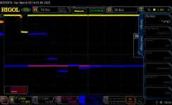
Next problem was the converter was saying it was done after second clock pulse. The A/D is Successive-approximation. You can select between 6 and 12 bit of resolution at 166k to 18k conversions per second by connecting pin PE12-J to the correct memory buffer bit (MB) and adjusting the R401 clock frequency. The more bits the slower the clock needs to be for the signals to settle to the 1/2 LSB resolution. The computer is using the MB as a shift register shifting a one across with each clock. The connection was supposed to be to the active high signal but it was connected to the active low signal. I unwrapped the wire and jumpered it to the correct pin. The A/D converter never finished conversion since the one wasn't being shifted in. Found that the A/D converter depends on a R123 card that is listed as part of the 681 data line interface option. The module location chart is missing marking that card as part of the A/D also. The manual referred to the R123 at PC5 but its really in PE5. I didn't have a R123 with me so will need to wait till next visit to finish. I have some push on pins that I'll put on the wire that selects the number of bits so it can be easily changes in the future. The not installed 681 option allows the PDP8 to interface to a 685 serial line multiplexor to talk to up to 128 teletypes. This machines has the normal single teletype interface installed.
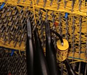
Machine also has this cap on PE12 delay card. Its not documented in the manual. Manual says delay should be 1/2 microsecond. With cap I think it was 40 microseconds. It looks like a later addition. The red sleeving around the pin looks like they put that in to try to prevent melting nearby wires when it was soldered on. Suspect I'm going to need to remove it.
Still need to figure out what we want to connect to A/D to demo. The computer has 4k 12 bit words of non volatile core memory and no mass storage. All output needs to be teletype or accumulator lights.
I put my Debounce card in the machine to make the front panel work better. Closed the machine up and checked the demos we leave in core. The text punch wasn't working properly. Tried to reload from paper tape and that made it worse. Code was getting loaded to the wrong location. Looked like carry wasn't working between some of the R211 cards. Wiggled the R211's and problem cleared up so we still have an intermittent connection which will need to wait for next time. Reloaded the demos and verified they all worked then headed home. Looking closer at the badsolder picture some other solder joints look suspect. Will test better next time. I had one bad solder joint in my 8/I on power bus strip like this. Hopefully won't start getting a lot of this problem.

And got the expected result after going through all the effort of no change in symptoms. Tried brushing hand over wirewrap pins on those cards and it triggered incorrect operation. Sometimes one of the memory address register bits didn't seem to load with examine switch. Inspecting that pin I could see a bad solder joint where they had used a bus strip to connect pins across all the R211 cards. See pin where the red clip is on. That is pin PC16-M which is PC->MA (Transfer program counter to memory address register). You set the PC to address you want to read with load address then examine switch transfer it to MA register to read memory and increments PC.

Didn't think I could resolder without damage to wires to added a purple wirewrap to the next pin. Could then wiggle cards and pins without crashing the moving light demo.
Next was working on the A/D converter. It looked like the machine originally didn't have that option installed. Likely the The R.E.S.I.S.T.O.R.S. got the cards and installed them but it wasn't in a working state. The manual said you just had to install the cards but it looked like you had to also remove some wires to enable it. VCF management agreed that it was ok to remove the wires to enable the A/D converter.
I started troubleshooting the converter. First issue was the R401 card in PE13 wasn't generating the conversion clock. I replaced a bad diode on the card to fix. Most of the logic in the PDP-8 is done with discrete diodes.
Next issue was the memory buffer register wasn't shifting. The shift signal from the A/D converter was grounded to prevent noise pickup when the A/D wasn't installed. They used red to mark the wires that needed to be removed to install options. Not sure what orange and green wires signify. I removed the wire from MB SHIFT (pin DU). Also removed ground from AC R210 A-D CONV (pin BP). In the picture you see other red wires. Will see if they are for A/D or other peripheral not installed.


Next problem was the converter was saying it was done after second clock pulse. The A/D is Successive-approximation. You can select between 6 and 12 bit of resolution at 166k to 18k conversions per second by connecting pin PE12-J to the correct memory buffer bit (MB) and adjusting the R401 clock frequency. The more bits the slower the clock needs to be for the signals to settle to the 1/2 LSB resolution. The computer is using the MB as a shift register shifting a one across with each clock. The connection was supposed to be to the active high signal but it was connected to the active low signal. I unwrapped the wire and jumpered it to the correct pin. The A/D converter never finished conversion since the one wasn't being shifted in. Found that the A/D converter depends on a R123 card that is listed as part of the 681 data line interface option. The module location chart is missing marking that card as part of the A/D also. The manual referred to the R123 at PC5 but its really in PE5. I didn't have a R123 with me so will need to wait till next visit to finish. I have some push on pins that I'll put on the wire that selects the number of bits so it can be easily changes in the future. The not installed 681 option allows the PDP8 to interface to a 685 serial line multiplexor to talk to up to 128 teletypes. This machines has the normal single teletype interface installed.
Machine also has this cap on PE12 delay card. Its not documented in the manual. Manual says delay should be 1/2 microsecond. With cap I think it was 40 microseconds. It looks like a later addition. The red sleeving around the pin looks like they put that in to try to prevent melting nearby wires when it was soldered on. Suspect I'm going to need to remove it.

Still need to figure out what we want to connect to A/D to demo. The computer has 4k 12 bit words of non volatile core memory and no mass storage. All output needs to be teletype or accumulator lights.
I put my Debounce card in the machine to make the front panel work better. Closed the machine up and checked the demos we leave in core. The text punch wasn't working properly. Tried to reload from paper tape and that made it worse. Code was getting loaded to the wrong location. Looked like carry wasn't working between some of the R211 cards. Wiggled the R211's and problem cleared up so we still have an intermittent connection which will need to wait for next time. Reloaded the demos and verified they all worked then headed home. Looking closer at the badsolder picture some other solder joints look suspect. Will test better next time. I had one bad solder joint in my 8/I on power bus strip like this. Hopefully won't start getting a lot of this problem.

