Roland Huisman
Veteran Member
Hi Doug,
Okay, good to know. You can check it better on that board.
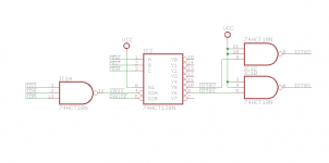
The 8881 = 7439 can do 60mA at the output. But the bus is only pulled up for max 15mA.
(1K pull up at 15V limited by diode to limit on 3V. This is done to get a higher slew rate on the bus)
The higher current output chips have the strength to pull that 15mA to a really low level.
Since the 7401 is pin compatible with the 8881 and 7439 I would place one of these for testing.
If you want I can sent you a 7439 or an 8881 for shipping costs. But I don't know how things
are now regulated with shipping to the US...
Regards, Roland
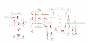
I have the M840K revision also. And that cap is C65 on the diagram which goes across the 4 diodes in series. It is definitely installed backwards.
Okay, good to know. You can check it better on that board.
How much could the 8881 do? I guess if you needed more drive you could sub a 74S38 since it can drive 60 ma. It doesn't look like the higher speed should be an issue on the application on this board.
The 8881 = 7439 can do 60mA at the output. But the bus is only pulled up for max 15mA.
(1K pull up at 15V limited by diode to limit on 3V. This is done to get a higher slew rate on the bus)
The higher current output chips have the strength to pull that 15mA to a really low level.
Since the 7401 is pin compatible with the 8881 and 7439 I would place one of these for testing.
If you want I can sent you a 7439 or an 8881 for shipping costs. But I don't know how things
are now regulated with shipping to the US...
Regards, Roland
") .
.