• Please review our updated Terms and Rules here

XT-FDC project level of interest

A quad flat package is easier to solder by hand then a ball grid array.
Although i must admit it's not for the faint of heart nor for those without a good soldering station.

Although If we do go this way I propose dropping the second ROM socket since it would become redundant with a CF onboard.
 
The FDC37C669 looks idea - but being QFP/TQFP, I'd be nervous that it could limit the appeal of the project. Unless a short-run of 669s-on-through-hole-breakout-boards is the thought?

James, that's an odd comment for someone who has just produced an SMT CF disk controller, isn't it? :)
 
Ha, yes that's true at first sight. But I believe the SMT issue has muted demand (I've shipped maybe 10 PCBs only, yet PCBs have been available free of charge, BoM is about $12, and it's nearly twice as fast as any other XT compatible disk controller). I'd hate to see this project fail for the same reason.
 
There's always an ATF1508. Cumbersome, but I'll spin a prototype now that your PLD code is stable and tested. I have a working XT-IDE ATF1508 board design, but during early testing showed more device compatibility problems than both earlier designs.

There is also taking a few useful SMT components, placing them on a mezzanine card or a full card, then starting a kickstarter to pay for fab. Removes the hobby assembly requirement from the equation.
 
But I believe the SMT issue has muted demand (I've shipped maybe 10 PCBs only, yet PCBs have been available free of charge, BoM is about $12, and it's nearly twice as fast as any other XT compatible disk controller).

I don't know if it may be the case with others, but for me, it's not the SMT that's the problem, rather, it's the fact that I didn't know about it. I mean, I was vaguely aware that the project existed, but did not realize that it was functionally superior or that it had even progressed to the point that boards were publicly available. Now that I go back and look, I see the big long thread about it, but until now I'd assumed that was just another thread about the 'other' XT-IDE.
 
I can remember going from point-to-point wiring using my Weller 225-watt gun to PCB, thinking "everything is so tiny here--I'll never get it". I really don't know how to cope well with BGA, but TQFP isn't a big deal anymore for me. Like anything else, it's an acquired skill, I suppose.

You could use a mezzanine board if it helps, but the hassle of 100 pins still is going to bother some folks, even if it's rigged out to 25 per side of a square adapter board. Schmartboards has some easy-to-work-with adapters that aren't hideously expensive.
 
Hi Andrew,

Here's what's on my list:

  1. Fix the bit A7 decoding for the I/O port.
  2. I can give you exact positions relative to the ISA edge connector; will that do for the external connector? (I need a reference point)
  3. The second internal drive connector P2 needs to be moved a bit away from the external (DC37) position--otherwise, there's too little clearance if both are installed.
  4. The 50-pin 8" header needs to be moved over as well (too close to the bracket side of the board.
  5. Add some space between the crystal/10 pF caps (C12/13) and the PLCC pads so that there's clearance for them after a PLCC socket is installed.
  6. Put some distance between JP11 and P18.
  7. Drop the DP8473 and associated components.
  8. Adding some 74LS07 drivers (do you want to add receivers) might give a little protection.
  9. Very minor, but I hate to see Vcc on a jumper pin--too much possibility for mayhem. Can K9 be made a simple 2-pin affair that simply grounds a pulled-up pin?

Has anyone else built up their board?

Hi Chuck! OK, I'll keep this list as the reference for when I update the PCB. Hopefully the other builders can get theirs made as well so we can shake out any other bugs. My plan is to have all the prototype boards built and tested and then update the PCB to incorporate all the feedback.

Thanks and have a nice day!

Andrew Lynch
 
Just curious. Will the XT-FDC be capable to coexist in machines with integrated FDC? Both Commodore PC10-II as well PC10-III have on board FDC for DD drives (360kB/720kb).
 
Well, perhaps as secondary controllers; that is, using a different port (and perhaps IRQ and DMA) with an appropriate driver, but if the primary integrated controller can't be disabled, you won't be able to boot from the XT-FDC. We did include prinary/secondary address jumpers and also selectable IRQ and DMA, but plans for the BIOS ROM only call for supporting boot as the primary controller.
 
Hi Chuck! OK, I'll keep this list as the reference for when I update the PCB. Hopefully the other builders can get theirs made as well so we can shake out any other bugs. My plan is to have all the prototype boards built and tested and then update the PCB to incorporate all the feedback.

Thanks and have a nice day!

Andrew Lynch

Andrew - can you fill out that list of changes (and any others you have received) to make it more idiot proof? I'm assembling the parts collection that I need to start assembly and would like to know about all of the required changes up front.

(I'm late on building - that's a whole different story .. but it's getting closer.)


-Mike
 
Hi Mike! Thanks! The only "cut and jumper" we have so far is the problem with the IO decoder logic. Pin 16 of U6 should be GND instead of VCC. It would be a lot easier to cut that in on the PCB before any sockets are installed. The rest of the changes are basically moving things around and adding the additional buffering.

Thanks!

Andrew Lynch
 
Here's my card presently:

Main FDC (PC8477B)

I ordered the wrong PLCC socket. Awaiting proper socket. Once I have that, I can test.

Alternate FDC (DP8473V)

Earlier posts indicate that this is to be 'dropped'. Won't go any farther with it.

Optional Boot ROM (28C64)

Tested good.

Optional ROM Drive

Parts arrived. I will start testing this. That doesn't mean writing code to go into the AM29F040 Flash Memory. I will test the ability to flash, and the ability to individually address/read the 64 by 8K sized pages (checking that one page does not affect any other).

8" Floppy Drive Connector

I will investigate this once I have the 'Main FDC' section going.

xt-fdc_at_20oct12.jpg
 
Here's my card presently:

Alternate FDC (DP8473V)

Earlier posts indicate that this is to be 'dropped'. Won't go any farther with it.

Thanks for the update! Very encouraging! Now all the builders should have their PCBs and have build and test underway. Please post results as they come available. Obviously Chuck is way ahead since he received his board first.

Dropping the DP8473 is still under consideration. If it works it may be worth keeping it. Just leave the pads DNP assuming it does not adversely impact the proper operation of the primary PC8477B FDC choice. I would like to preserve as much hobbyist flexibility as possible to allow for the unique options the DP8473 provides and also as a hedge against parts non-availability.

I very much appreciate your effort. Thanks and have a nice day!

Andrew Lynch
 
Dropping the DP8473 is still under consideration. If it works it may be worth keeping it. Just leave the pads DNP assuming it does not adversely impact the proper operation of the primary PC8477B FDC choice. I would like to preserve as much hobbyist flexibility as possible to allow for the unique options the DP8473 provides and also as a hedge against parts non-availability.
Okay then.
 
Page 50 of the National Semiconductor PC8477B datasheet contains, "In this design we have used 1k pull-up resistors on the floppy drive interface. If the intended design is to be used with external drives or long cabling, or if 5.25" disk drives are to be supported, 150k pull-ups should be considered."

The prototype is using 1k. Has there been any discussion as to whether or not 150k should be used? I note that the manufacturer used "should" rather than "shall" or "must". Clearly, there is a compromise between the use of 1k and 150k, otherwise the manufacturer would have stipulated 150k only. One of the lines affected is READ DATA.

I guess that if all of the testers don't encounter issues when 5.25" drives are used, then 1k is acceptable. But perhaps the use of 1k may result in intermittent problems, not picked up during testing. It suggests that 5.25" drive testing may need to be somewhat rigorous (e.g. random read/write test over a few hours).
 
If the NSC doc says 150K, that's a typo. It should be 150 ohms. That's nominal for both 8" and 5.25" drives, but 1K should work fine, unless the cabling is in excess of about 1m. I suppose you could compromise at 470 ohms.
 
If the NSC doc says 150K, that's a typo. It should be 150 ohms.
It should have hit me that a 1:150 contrast was too high.

That's nominal for both 8" and 5.25" drives, but 1K should work fine, unless the cabling is in excess of about 1m. I suppose you could compromise at 470 ohms.
Let's see how the testing (from all testers) goes.
 
Optional ROM Drive

Per the following, 4 of 6 tests were completed.
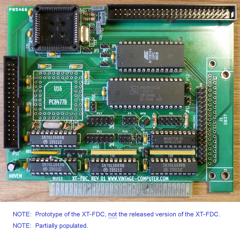
I need to work out now how to flash the AM29F040 (fitted to XT-FDC) from DOS.


-----------------------------------------------------------------------------------
TEST 1: ADDRESS TEST 1 oF 2

a) Created an 512 KB binary file, where:
* First 8 KB block filled with byte 00
* Second 8 KB block filled with byte 01
* Third 8 KB block filled with byte 02
...
* Last 8 KB block filled with byte 3F (63 decimal)

b) Using an EPROM programmer, flashed that file into an AM29F040 chip.

c) Fitted AM29F040 to XT-FDC.

d) Set P5 jumpers and JP7 for a ROM base address of C8000.

e) Verified via a custom DOS program that each 8 KB block ('selectable ROM') in the AM29F040 read as expected. The pseudo code was:

for each of the 63 'ROMs'
{
select the 8KB ROM .............. (comment: via an appropriate write to port 3F6h )
read entire 8KB ROM contents
report error if any byte read not the same as the ROM # (e.g. ROM #4 [logical] expected to contain bytes of 04 )
}


f) Using an EPROM programmer, changed one byte in the AM29F040.
g) Verified that my code detected that byte (i.e. in order to partially check my program's integrity).

-----------------------------------------------------------------------------------
TEST 2: READ DATA TEST

a) Using an EPROM programmer, modified first 18 bytes of AM29F040 to be:
00 / FF
01 / 02 / 04 / 08 / 10 / 20 / 40 / 80 (walking one)
7F / BF / DF / EF / F7 / FB / FD / FE (walking zero)

b) Fitted AM29F040 to XT-FDC.

c) Via DEBUG, verified that the first 18 bytes were as expected.

-----------------------------------------------------------------------------------
TEST 3: ADDRESS TEST 2 oF 2 (BASE ADDRESS OF 'SELECTABLE' 8KB ROM)

One of the things verified by test #1 was the generation of /CE on the AM29F040.
But it was done only using one possible base address, as selected by jumpers on P5 and by JP7.

Checked the card at various addresses, verifying that:
* ROM appeared at the selected address; and
* ROM did not also appear elsewhere.

Addresses checked: AA000/C8000/CA000/CC000/CE000/D0000/D2000/E0000

-----------------------------------------------------------------------------------
TEST 4: ROM ENABLE TEST (JP8)

Verified that removing JP8 resulted in the ROM no longer being 'seen'.

-----------------------------------------------------------------------------------
TEST 5: FLASH TEST

<pending>

-----------------------------------------------------------------------------------
TEST 6: WRITE ENABLE TEST (JP9)

<pending>

-----------------------------------------------------------------------------------
 
Back
Top