• Please review our updated Terms and Rules here

Z280 homebrew board plan

bakemono

Experienced Member
Joined
Jan 19, 2020
Messages
212
Location
USA
Anyone want to comment on these schematics? Anything stand out as being horribly broken?

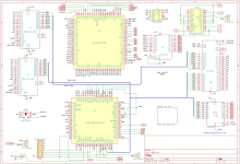
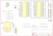
The plan is to have a Z280 in 16-bit ZBUS mode. An Altera CPLD acts as a 'chipset' to handle DRAM, PS/2 keyboard port, and signals for the 8-bit ISA slots. A 74373 latches/buffers some address lines. 74245 buffers some data lines. A MAX232 let's the UART connect to a DE-9 serial port. And there's an EPROM. 2x 1MB SIMMs would be installed, though bank switching would be needed to access the whole thing, since only 20 Z280 address lines have made it to the CPLD.

I'm thinking I'll be able to reprogram the CPLD in the board by using the jumper to tie the CPU's reset line low during the process. And if I run the CPU clock at something close to 14MHz then I can jumper that to go to the ISA OSC signal as well, rather than needing a separate crystal.

Originally I wanted to through everything and kitchen sink on there, but gradually tried to simplify it as much as possible while keeping the DRAM memory and ZBUS mode. I think I can route this on 2 layers but I'm not sure if it's even worth it to try. It seems that JLCPCB is offering cheap 4-layer boards now as well. I have not tried making a 4-layer board yet. Any thoughts?
 

Attachments

  • z280-1.png
    z280-1.png
    74 KB · Views: 20
  • z280-2.png
    z280-2.png
    51.5 KB · Views: 20
4 layer boards are wonderful. Keep the bottom layer nothing but a GND fill. No traces at all.
 
4 layer boards are wonderful. Keep the bottom layer nothing but a GND fill. No traces at all.
He's using KiCAD. The default stackup in KiCAD is (top to bottom): signal, GND, PWR, signal. No need to change it at these clock rates. Layout is simple: generally going North-South on one signal layer and East-West on the other with vias to switch layers and NO SIGNAL ROUTING ON INNER LAYERS. Then, when you realize you need to cut a trace and add a blue wire or two (dozen), you can do it. Because sometimes you don't notice that one manufacturer defines bit 0 as the least significant bit and another one defines it as the most significant bit o_O

blue wires.png
 
He's using KiCAD. The default stackup in KiCAD is (top to bottom): signal, GND, PWR, signal. No need to change it at these clock rates. Layout is simple: generally going North-South on one signal layer and East-West on the other with vias to switch layers and NO SIGNAL ROUTING ON INNER LAYERS. Then, when you realize you need to cut a trace and add a blue wire or two (dozen), you can do it. Because sometimes you don't notice that one manufacturer defines bit 0 as the least significant bit and another one defines it as the most significant bit o_O

View attachment 1264097
I had a very similar thing happen to me - on every datasheet in the world the pad view is top view . . . except 1 obscure audio chip. Ask me how I know :)

Also, I agree with the above layer stackup, that's not how I learned it but it makes far more sense.
 
I decided to reroute an interrupt line so the keyboard can generate an interrupt, and to connect the ISA slot refresh signal in case my VGA card needs it.

As to what I'm going to use it for, I'd say 1) experimentation 2) amusement 3) adding more stuff to my order, since I'll already have paid the shipping cost for some other boards I need.
 
It'll have to load stuff from a remote system (via serial, etc.) or I'll implement something on an ISA card down the road.
 
Nope, this is the first I've heard of an STD bus (insert joke about public transportation in one of our less clean cities). The picture on wikipedia looks like something I may have run across though. I wonder if they were used in old packaging machinery.
 
first signs of life from this, in the form of some blinking LEDs
Right now the 7128 is just directly feeding a pair of instructions to the CPU. The instructions load the A register, and write it out to I/O port $80 which is then reflected on the LEDs. I think I have a mis-routed signal that needs to be fixed before I can boot from ROM. DRAM controller still needs to be implemented in the CPLD also. But I'm glad to have some measurable activity and a lack of smoke.
 
Looking good. CPLD should have enough logic to do DRAM controller, CF interface, and I2C/SPI etc. This is my version of Z280 operating in ZBUS mode, Z280RC. It is ROMless and bootstraps from CF disk. It is 2-layer pc board, but if I were to design it today, I'll go 4 layer because DRAM is noisy and 4-layer is so cheap now. CP/M and RSX280 are ported to it.

You may also be interested in a Z280 emulator.

BillZ280RC_annotated.jpeg
 
Hi Plasmo, I saw a post about one of your earlier boards a couple years back. Didn't know you were also working on a ZBUS version! Are there any interesting secrets you've discovered about the Z280 that may have been missing or wrong in the documentation?
 
hperaza has published a buglist for Z280 on retrobrewcomputers.org forum here, https://www.retrobrewcomputers.org/forum/index.php?t=msg&th=742&start=0&

It is mostly software bugs. I know of one hardware bug dealing with metastable problem with CPU and UART clocks. The fix is to use one clock for Z280 and UART.

You may be interested in this long discussion (600+ replies) about Z280, https://www.retrobrewcomputers.org/forum/index.php?t=msg&th=93&start=0&

Another extensive Z280 info is by agn453 on github: https://github.com/agn453/Z280RC

I have Z280 designs for both 16-bit ZBUS as well as 8-bit Z80 compatible mode.
Bill
 
Hi Plasmo, I saw a post about one of your earlier boards a couple years back. Didn't know you were also working on a ZBUS version! Are there any interesting secrets you've discovered about the Z280 that may have been missing or wrong in the documentation?
Plasmo's Z280RC is emulated by z280emu. Plasmo has done several Z280 boards including both Z80 bus and ZBUS modes.

Plasmo's already pointed to the thread I started on retrobrew computers that resulted in reviving Tilmann Reh's excellent CPU280, a ZBUS Z280 with up to 4MB of burst-mode DRAM, RTC, and FDC on an ECB bus card. I still have a handful of blank boards. But Plasmo's design is easier and much less expensive to build than CPU280. But the CPU280 at this point qualifies as a vintage CP/M machine.
 
Back
Top