| VCF West | Aug 01 - 02 2025, | CHM, Mountain View, CA |
| VCF Midwest | Sep 13 - 14 2025, | Schaumburg, IL |
| VCF Montreal | Jan 24 - 25, 2026, | RMC Saint Jean, Montreal, Canada |
| VCF SoCal | Feb 14 - 15, 2026, | Hotel Fera, Orange CA |
| VCF Southwest | May 29 - 31, 2026, | Westin Dallas Fort Worth Airport |
| VCF Southeast | June, 2026 | Atlanta, GA |
-
Please review our updated Terms and Rules here
You are using an out of date browser. It may not display this or other websites correctly.
You should upgrade or use an alternative browser.
You should upgrade or use an alternative browser.
ZX81 keyboard decoder
- Thread starter bbcmicro
- Start date
Are you trying to do a replacement keyboard?
I don't have the exact layout, but it was laid out as four rows and something like 9 or 10 columns. Making a contact at the intersection of a row and column generated a keypress. Very primitive, and easy to interface too.
Of course the downside is that the machine is always having to poll the keyboard interface. On something like an IBM PC an entire micro-controller in the keyboard is used for that purpose, freeing up the 8088 for more useful work.
Elar
Member
Here's the schematics for ZX81:
http://www.ts1000.us/files/ts1000schematic.pdf
http://www.ts1000.us/files/ts1000schematic.pdf
ahm
Veteran Member
Back in the day, I added a full sized keyboard (with reed switches!) to a Timex, only to discover that it wasn't the junky membrane keyboard keeping me from being able to type as fast as usual, but the slow keyboard scan rate in the machine.
80sFreak
Experienced Member
Back in the day, I added a full sized keyboard (with reed switches!) to a Timex, only to discover that it wasn't the junky membrane keyboard keeping me from being able to type as fast as usual, but the slow keyboard scan rate in the machine.
Doesn't life suck sometimes?
")
Cheers,
80sFreak
ahm
Veteran Member
Doesn't life suck sometimes?
It is what it is.
carlsson
Veteran Member
bbcmicro: If you're interested, I have a few different computer magazines describing how to build your own keyboard, memory expansion etc to a ZX-81. The articles unfortunately are in Swedish, but perhaps it would help you a bit if you can't find similar articles published in UK magazines.
ziloo
Veteran Member
ZX81 stuff!
ZX81 stuff!
bbc,
I have found these links very informative: uke:
uke:
http://www.zx81.de/webring/index.htm
http://zx81kit.co.uk
Hope it helps! :frankenstein:
ziloo :wave:
ZX81 stuff!
bbc,
I have found these links very informative:
uke:http://www.zx81.de/webring/index.htm
http://zx81kit.co.uk
Hope it helps! :frankenstein:
ziloo :wave:
carlsson, I would appreciate the magazines. I need as much info as I can get because although it seems that a simple replacement of the existing keys, wired up using the same matrix and just a pin-for pin replacement is susceptible to problems. I read somewhere that an extension of the keyboard is subject to somethingbad to do with signal degradation or something. It had an important sounding name but I can't remember what it was. I also need to look into deboucing and look that up, but I seem to recall that the limeted speed on the keyboard mentioned by ahm was because the processor was taken up deboucing, choosing the middle signal or strongest (not sure how it works) from the many recieved on a keypress.
I wish to know out of an avid interest, with the idea to replace the keyboard in the future.
Thanks.
I wish to know out of an avid interest, with the idea to replace the keyboard in the future.
Thanks.
carlsson
Veteran Member
At the moment I can't access my scanner, due to I've stored away all my furniture and some boxes with assorted cables including the USB scanner cable! Perhaps in a month or so I will get the stuff back and be able to scan the articles in question. I suppose you're not in a great rush?
ziloo
Veteran Member
Well bbc,
you know what they say... "Whenever you want something, think very carefully because you may get exactly what you asked for..."
I hope these links will provide you with what you are asking for :icecream::
http://www.user.dccnet.com/wrigter/index_files/ZXKBDv3.htm
http://www.user.dccnet.com/wrigter/index_files/ZXATKEY.htm
Have fun :cool1:!
ziloo
Veteran Member
I need to construct a keyboard replacement. The membrane keyboard is totally dead, despite best repair efforts. I know the keyboard circuitry is fine because crossing points with a jumper on the motherboard connectors outputs characters on the screen.
I have found hazy descriptions of the keyboard matrix on the internet but I really need a simple schematic of one. I have cut down an old mechanical keyboard and it now just has the keyswitches on it. I have soldered a long IDE connector to the reverse of the keyboard sockets on the motherboard. All I need now is to solder a matrix and I'm finished, but I can't get adequate info. I get a metal block working from descriptions, I can't hold it all in my mind.
So, can anyone help me?
I have found eough infor on the column and row layout, but I'm still confused.
The keyswitches have two poles, right? Push the key and the contacts meet and the current goes through.
In most schematics the keys are illustrated as this:

So how do I solder four wires to two poles? What's the arrangement?
I realise I am being a bit dense.
The keyswitches have two poles, right? Push the key and the contacts meet and the current goes through.
In most schematics the keys are illustrated as this:
So how do I solder four wires to two poles? What's the arrangement?
I realise I am being a bit dense.
nige the hippy
Veteran Member
yo beeb,
It's just shorthand, the key is at the intersection between row & column, push the key, and it connects that row to that column.
incidentally... circuit diagrams...
a solid line represents a connection
a junction is shown by a dot on the junction
if two lines cross, they don't connect (unless there is a dot, and it's usual to show 4 wires connecting as a staggered junction (2 tees close to each other) rather than a crossroads with a dot, saves confusion)
And I haven't forgotten.... just STUPIDLY busy
Right, now I understand that, how do I implement it? I've spent most of my day head-scratching over this; soldering bits, testing, scrapping and goto 10
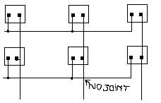
Lets play a game.
Here is a representation of a simple 3x2 matrix

Ok, I follow that pushing a switch makes its' row and its' column connect and sends its' coordinates in a manner of speaking, to the ZX81 CPU which then decodes the cordinate (e.g. First column, second row = 1,2 = Q (I don't think it's that exactly)).
Now, can someone draw lines as a representation of where the wires connect physically on the back of the pcb, in the real world? It's the fact that there are four leads for every two conections that I can't get my head around. The first correct answer gets a gold star!
This is for my benefit, bear with me but I am a very visual person.
Fill in the blanks, so to speak.

BTW Nige, I forgot that I still have snow crash. PM me when you want it back.
Lets play a game.
Here is a representation of a simple 3x2 matrix
Ok, I follow that pushing a switch makes its' row and its' column connect and sends its' coordinates in a manner of speaking, to the ZX81 CPU which then decodes the cordinate (e.g. First column, second row = 1,2 = Q (I don't think it's that exactly)).
Now, can someone draw lines as a representation of where the wires connect physically on the back of the pcb, in the real world? It's the fact that there are four leads for every two conections that I can't get my head around. The first correct answer gets a gold star!
This is for my benefit, bear with me but I am a very visual person.
Fill in the blanks, so to speak.
BTW Nige, I forgot that I still have snow crash. PM me when you want it back.
Last edited:
nige the hippy
Veteran Member
( remember joints are dots, and where wires cross, it means that they go straight over)
ps. when it comes to reading computer diagrams, usually busses are represented by a thick line, with various (labelled!) thin wires joining and leaving, again it's shorthand for the electrical equivalent of a bundle of wires
pps
Just got a complete sirius1 for a fiver, fairly local pick-up") just have to tell wife, and make more room in the garage
just have to tell wife, and make more room in the garage
ps. when it comes to reading computer diagrams, usually busses are represented by a thick line, with various (labelled!) thin wires joining and leaving, again it's shorthand for the electrical equivalent of a bundle of wires
pps
Just got a complete sirius1 for a fiver, fairly local pick-up
just have to tell wife, and make more room in the garageAttachments
It's an epiphany!
It's an epiphany!
Thankyou so much Nig!
It was driving me mad. I can get back to it now, alythough I wish I had known it yesterday. I would have had all sunday then. Ah well.
As promised, here is your star.

Someone else always gets the bargains. Ah well, they always have cars.
It's an epiphany!
Thankyou so much Nig!
It was driving me mad. I can get back to it now, alythough I wish I had known it yesterday. I would have had all sunday then. Ah well.
As promised, here is your star.
Someone else always gets the bargains. Ah well, they always have cars.
fred3rd
Experienced Member
BBCMICRO
When you have the bugs worked out of your kb project, please post all details w/pics if possible. I just dove head first into the ZX81 world. I have found a lot of good links on it so far. One of my favorites so far is http://www.mainbyte.com/ts1000/index.html that has a link to http://www.mainbyte.com/ts1000/composite.html .
This link gives detailed instructions on how to adapt the ZX81 to use a composite monitor.