• Please review our updated Terms and Rules here

Help with Elston DM30-09BO VDU board

more info......The H scan circuit is very sensitive to to exact power supply voltage as it affects the width of the scan. The width looks basically good, though it might be a tad low. Even so this set has a width control. So there cannot be excessive voltage drop across that overheating resistor. It is worth checking the voltage drop across it with the DVM and then we can calculate the power in it and the current to the H scan stage tp see of it looks reasonable. Also check the exact value of the resistor, has it been replaced before ?
 
I located this Elston Document that you might want to download and keep.

Larry
 

Attachments

  • Elston_DM30_DM40.pdf
    1.1 MB · Views: 22
Interesting...

I changed those caps I have spares for: C301, C311 and C302. C309 is marked as a 1uF electrolytic but on the board it's a film capacitor (tiny square package). I have a spare electrolytic 1uF, but it hasn't made any difference.

I noted that the V-LIN control is working, but only affects the bottom part of the screen, where the vertical lines look correct. Does this tell you anything?

Could it be a problem with the TDA1170S (U300)? Is there a way to check it with the 'scope? What I mean is, if I probe around it, what waveforms should I see?
 
Last edited:
more info......The H scan circuit is very sensitive to to exact power supply voltage as it affects the width of the scan. The width looks basically good, though it might be a tad low. Even so this set has a width control. So there cannot be excessive voltage drop across that overheating resistor. It is worth checking the voltage drop across it with the DVM and then we can calculate the power in it and the current to the H scan stage tp see of it looks reasonable. Also check the exact value of the resistor, has it been replaced before ?

The set is getting power from a 12v PC-AT supply but I only see 11.1v before the resistor, then 9.43v after it. Previously, I was running it without loading the 5v rail from the PSU, this gave about 1v less on the 12v rail. With the improved voltage, I still see the vertical compression at the same point in the image; that is to say, correcting the power rail voltage hasn't improved matters as far as the generated image is concerned.

The replaced R478 resistor is a pull from the other Elston board I have, which is in the same location in the circuit and is also labelled R478 (the overall design is slightly different to the Kaypro VDU, having just one 555 timer in the horizontal stage). The pulled resistor is quite a bit bigger than the original (burned out) part (in physical dimensions), so is likely a higher wattage, and has colour banding brown, red, gold or 1.2R, which should be correct. However, it actually measures 2.6R which is likely due to it overheating (which it's still doing despite the horizontal circuit looking proper). I plugged the figures into a voltage drop calculator and it suggested 1-2 ohms is all that is needed to give this voltage drop, with a current draw of 1 amp. With an ammeter in series, the whole unit is only drawing 1.24A which does seem reasonable. Yet without the tube filament heater connected, it still draws 1.18A which surprises me because I'd have thought the filament would pull the lion's share of the current.
 
Last edited:
@gertk, I forgot to mention:

  • check C310 (DC decoupling cap for the vertical output, might be shorted, probably overloading/damaging U300).

I did change this over and it may well have been the fix for the horizontal circuit, but it's not the only capacitor I swapped in there. Unfortunately I'd inadvertently turned the brightness all the way down so I didn't see the effect of each of the replacements (also there was a bad connection on the HOT).
 
One adjustment that doesn't seem to have any effect is the B+ trimmer. What is it for and how should it be set?

[Edited to add] I did some googling about B+ and not sure where to attach a meter to test it, or what the expected voltage should be - maybe it's a spec of the LOPT or CRT? Anyway, it is marked as R503 on the board but it doesn't appear to be on the schematic. It is present in the DM40 schematic in the PDF that Larry linked to though:

R502 B+ adj.JPG
...but that's the 55v power rail adjuster in the DM40's regulated PSU. The regulator IC itself is U501 and there is a Q501 on the board, though nothing to indicate what it's there for. Q501 is a 2N5193 general purpose PNP power transistor, whereas U501 (on the DM40 schematic) is an LM317K, a 1.2v-37v adjustable regulator. Until I trace the circuit round this part I can't be sure what it's doing there.. but it seems more a coincidence that these semiconductors have the same number in both scematics.
 
Last edited:
The overall current looks about right. Generally I would expect the current into the H scan stage alone (that is fed by via resistor) to be about 0.7 to 0.8A, at worst perhaps 1A. So the power in the series resistor, worst case, would be 1.2W for that resistor. I think just replace the resistor with a 1 Ohm or 1.2 Ohm or 1.5 Ohm 2W rated metal film resistor, should be fine. Use the 1 Ohm if you want a tad more scan width compared to the 1.5 Ohm. If you used over 2 Ohm, you would need to go for a 3w rated resistor possibly. I would simply fit a 1 Ohm 2w part or the original 1.2 Ohm value if you can get one easily.

These small VDU's can run ok on 11V, provided the scan width is adequate and the width inductor slug doesn't need to be unscrewed too far to get the full width .

The next move now is to test the caps and or re-cap the area around the Vertical scan IC and see if you can fix the v scan linearity defect. If the problem is still there after the recap, we can look with the scope to try to work out why. Make sure the power supply rail right at the IC is ok and put the scope to check for any supply ripple there, but probably the IC's supply is ok.

The supply is at pin 2. But one of the very important IC pins is pin5 where the B+ supply is introduced via R318,CR301 and the capacitor C311. The reason is that this pin supplies the current to the bias diodes inside the IC which bias the power output devices (just like an audio amp). If the resistor had gone high or the diode defective, it could cause the kind of cross over distortion we are seeing in the V scan.

The electrolytics to check are C311,C301, C307,C309,C310. One method if you don't have an ESR meter for the initial check, you can simply parallel another of a similar value and observe the effect on the scan.

Even if the capacitors are ok, before the IC should be replaced all the resistors should be checked to, and the IC last on the suspect list because most likely, the reason there is a malfunction is that something has gone wrong with the IC's operating conditions, rather than the IC itself. And in this VDU, not much is being asked of this IC and its running only just above its minimum supply voltage.
 
Last edited:
....ps; one thing about the CRT heater currents, the values can be quite different depending on the CRT type. Typically for a 12V operated heater one might expect 300mA in a large industrial CRT, sometimes it is 150mA and for other CRT guns even lower. Sony for example made a 5" crt TV set with a 12V heater that only had a current of 70mA ! see pg 3 of this article:


Some manufacturers of VDU's placed a low value resistor in series with the heater. If the power supply rises quickly at turn on and has a low internal resistance, there can be a current surge in the heater circuit because when the heater is cold it has a much lower resistance than when hot, and the resistor helps limit the peak current, but generally when the heater is warm, the resistor would drop less than a volt.
 
Last edited:
The overall current looks about right. Generally I would expect the current into the H scan stage alone (that is fed by via resistor) to be about 0.7 to 0.8A, at worst perhaps 1A. So the power in the series resistor, worst case, would be 1.2W for that resistor. I think just replace the resistor with a 1 Ohm or 1.2 Ohm or 1.5 Ohm 2W rated metal film resistor, should be fine. Use the 1 Ohm if you want a tad more scan width compared to the 1.5 Ohm. If you used over 2 Ohm, you would need to go for a 3w rated resistor possibly. I would simply fit a 1 Ohm 2w part or the original 1.2 Ohm value if you can get one easily.
As the part fitted has been stressed and is now reading over the required 1.2 Ohm, (I measured it out of circuit at 2.6 Ohm) is it likely this (in bold, above) is why it is still overheating..?
 
Make sure the power supply rail right at the IC is ok and put the scope to check for any supply ripple there, but probably the IC's supply is ok.
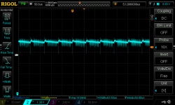
Waveform at pin 2 of U300:

U300  power rail.png

That looks a bit messy to me... C301, which I guess is to provide some smoothing to U300's power line, has been changed. However, I could try a bigger capacitor there to try and get it smoother. [Edit: Nope, no difference!]
 
The electrolytics to check are C311,C301, C307,C309,C310. One method if you don't have an ESR meter for the initial check, you can simply parallel another of a similar value and observe the effect on the scan.
All replaced, as well as C303 and C306 as they are in the V-LIN adjustment circuit. Interestingly, C309 is a film capacitor but on the other Elston board it's electrolytic. As I have a new electrolytic capacitor of the same spec I fitted it.

Unfortunately there is no improvement to the picture.

Even if the capacitors are ok, before the IC should be replaced all the resistors should be checked to, and the IC last on the suspect list because most likely, the reason there is a malfunction is that something has gone wrong with the IC's operating conditions, rather than the IC itself. And in this VDU, not much is being asked of this IC and its running only just above its minimum supply voltage.

There must be a way to look at the inputs of the TDA1170 in order to determine which resistor might be off or flaky. Failing that, a preferred order to replacing them? I'd hate to have to replace them all - so far it feels like a bit of a wild goose hunt and the board is very awkwardly connected to the tube so is a bit difficult to work on, especially the horizontal section. I have not removed the HT lead from the tube as it's neatly sealed with dielectric grease, so it's getting in the way.

I've swapped out the TDA1170 just in case, and you're right, it's not the problem. I'm getting to the "pulling my hair out" stage - if I had any to pull out, ha ha!
 
Last edited:
The operating conditions of the ic are listed in its data sheet which may help

Not so much - I don't really understand it, or rather how it relates to the conditions on my board.

Meanwhile, I've traced the V-SYNC from the Kaypro and through the circuit at Q298, which is missing - it's actually bypassed by a jumper cable. I thought to replace C300 but agin, no luck. I've tried a second PSU, thinking the first was a bit rough around the edges (some noise on the 12v rail) and it has not helped.

One thing I am struggling to understand is the V-Sync pulse. It looks completely stable at 59.5 Hz (about expected for a US monitor). But the picture is squished some way down. I expected a corresponding squish in the pulses.. but I realise now that the V-Sync comes once a frame. So what is driving vertical advance of the scan lines? I mean. I know the horizontal circuit is doing left to right scanning, but what part of the circuit is advancing the scan line to the next row?
 
Last edited:
One more thing, I replaced C308 and C312. C312 on the board differed from the schematic (1nF instead of 300pF) so I used a 300pF. These replacements made no difference to the picture. So, I seem to have replaced every cap in the vertical section to no avail.

Here's a test image which I knocked up in GWBASIC. Just rows of dashes, but the top is where the image is stretched most, then the second line is where it is compressed most, then the GWBASIC menu is where the image is normal.
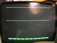
test pattern.JPG

Take a look at the waveform at TP2, which seems to show the raster structure from the vertical scan perspective.
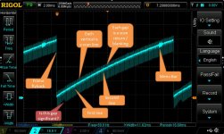
raster frame structure.JPG

I can see where the three rows are, and the vertical lines that look to me like noise on the ramps must correspond to each of the visible scan lines; then, at the top of the ramp we have the frame flyback (big vertical line dropping, ready for the next frame). Am I interpreting it correctly?

If so, I would expect to see the scan lines well spaced out at the start of the frame, getting closer together around the position of the second line, then spreading out to normal thereafter, but it doesn't seem to be the case. I've zoomed in and I can't see any tightening of the timings between the lines. Which in turn implies the TDA1170 is doing its job properly, but something else isn't.

There are some shorter scan lines at the start of the frame (highlighted in red), is this normal? Front porch?

It looks like a bad cap somewhere, but I have replaced many of them: C310, C301, C311, C302, C307, C309, C303, C306, C300, C308, C312. I think that is all the Vertical Section caps replaced now.

Looking at TP3's waveform, I think there is a correlation between the ramp down and the image, just like TP2, only this time the gradient is changing in a way that seems to mirror the compression of the image. Does that make sense?
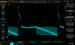
TP3 zoom.png
 
Yes, the last image above, TP-3 shows exactly what you would expect, for the screen image scanning defect. (ignore the superimposed H rate pulses, these are often seen with cross coupling of the yoke coils, though interestingly the level is higher than usual and different for the first half of the scan than the second half it probably represents the output impedance being different for each half due to IC failure).

Between the flyback pulses, there should be a gradual drop in voltage, like an inverted sawtooth with a slight curve in it. This voltage is generated by the sawtooth generator in the IC and based on slowly charging and rapidly discharging the timing capacitor.

So TP-3 should look a lot like an upside down version of TP-2, except with the high vertical rate positive going flyback pulses in it. As you can see from the recording the rate of change of voltage with time goes to almost zero near the center, so the beam spends more time there and that is why the beam brightens up there and is seen as a brighter horizontal few lines and above that the H scan lines are crushed together in the raster.

Assuming the resistors & caps are ok, it points to the IC itself as it looks like half of its output stage is not working properly.

Before replacing (the IC) just disconnect the yoke and make sure that there is no continuity between the H & V yoke coils, just in case. Also make sure to check the diode CR301. Also, a very important resistor to check, though you have probably done it, is the 1.5 Ohm current sensing resistor in series with the V yoke coils as this provides feedback to the IC to help control the scan linearity, but likely it is ok.
 
Last edited:
I located this Elston Document that you might want to download and keep.

Larry
Interesting to see the variations of the schematics with 3 x 555 monostables and the Vert deflection IC running of 24V rather than 12v. I wonder if these versions had larger CRT's than the one Jon is working on, probably by the look of the EHT voltage. The document is quite good as far as they go, giving a reasonable description of the function of the H scan stages.
 
As the part fitted has been stressed and is now reading over the required 1.2 Ohm, (I measured it out of circuit at 2.6 Ohm) is it likely this (in bold, above) is why it is still overheating..?
Assuming a fairly constant current for the H scan stage (its not constant and will drop a little with slightly reduced supply voltage), the power dissipated in the resistor is I^2 x R. So if the resistor value is increased it will run hotter. For example if you replaced that resistor with a link wire of near zero Ohms, you would not feel that link wire warm up at all. So the 2.6 Ohm resistor would likely run twice as hot as a 1.2 Ohm resistor. The actual temperature the resistor gets to though, for any power dissipation, depends on its its physical size as the resistor body has a thermal resistance (much like a heat sink) so the bigger the physical size of a resistor the cooler it will run for the same dissipated power.

A scenario like this can be a little confusing because obviously the resistor value, if increased large enough, would run cooler again as the current would drop very low.

In fact the maximum heat that can be generated in a resistor occurs when the resistor value is equal to the internal resistance of the supply, or that of another load in series with the supply, if the supply resistance itself is very low . It is a similar scenario in AC circuits, audio amps for example, where say the maximum power that can be delivered to a load occurs when the load impedance matches the amplifier's output impedance.

You can check this out just a simple model with a 10V DC power supply and a series 10 Ohm resistor. You have created a 10V supply with an internal resistance (or output resistance) of 10 Ohms.

If you play around with different resistor values loading this supply, the maximum power you can get into the load resistor you add occurs when it is also 10 Ohms, equal to the internal resistance of the supply you have created. Obviously when it is zero Ohms you can't get any power dissipated in the load resistor you add, and when it is infinity Ohms, no power either.
 
Last edited:
Sorry I did not see you had swapped out the IC already,
Do those other checks I mentioned on the diode & yoke ,we will get to the bottom of it.

There is something else you could test. Notice how the two vertical yoke coils are in series. There is usually a tag on the yoke where the two coils join up. See if you can measure the DC resistance of each separate coil, they should be practically identical.
 
Last edited:
Back
Top