• Please review our updated Terms and Rules here

Help with Elston DM30-09BO VDU board

JonB

Veteran Member
Joined
Jan 26, 2014
Messages
1,652
Location
South Herefordshire, UK
Hi

I'm trying to repair a monochrome video board from a Kaypro 16, made by Elston. It's a DM30-09BO. It was working for a short while, then yesterday a resistor started smoking and it died.

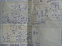
@ldkraemer was kind enough to send a schematic which I reproduce below. The smoked resistor is the 12R 2W R478 which sits between +12v and the board (the tube filament heater is also connected but direct to the PSU, not going through the resistor). What is the purpose of this resistor? Is it current limiting to protect the circuit in case of failure such as I have? The fuse, also inline, has not failed.

At the moment, it will power up the tube filament but there is nothing on the screen. However, a reset of the Kaypro causes a faint horizontal line to be displayed which fades out to a dot. All the while, the resistor is heating up... but I see no evidence of other components getting hot and I don't really want to touch anything to check for heat.

Seems like something is pulling too much current...

Is there anyone here who can advise on how to diagnose and repair this board?
 

Attachments

  • Elston DM30-09 schematic.JPG
    Elston DM30-09 schematic.JPG
    265.4 KB · Views: 52
R478 is a 1.2 Ohm resistor, probably a 'fusible' resistor (meaning it can burn through like a fuse without causing much damage to the surrounding area). It restricts the maximum current going into the horizontal output stage.

You have to check for shorted/worn components in circuit beneath R478( did F401 not blow ?)

Check components:
Q414 (horizontal output transistor)
C438 (filter capacitor over Q414)
C440 (electrolytic capacitor)
C439 (electrolytic capacitor)
CR407 (High Voltage! rectifier/diode, you can not measure this with a multimeter!)
CR408 (step-up diode for boosting the horizontal output transformer supply voltage)
CR409 (focus voltage rectifier)
C486 (focus voltage filter capacitor)
C441 (note this is a non-polar electrolytic capacitor, not easy to get)

Also since you mention you see a faint horizontal line sometimes, it could mean the short/overload is happening in the vertical output (follow the 'TO "A" +12V' path. Check the voltage there, if less than 12V there is some overload going on (but then F401 would blow unless it has been replaced by some inappropriate value)

Likely candidates in the vertical output stage (I am getting a dejavu here...)

U300 (TDA1170S, try desoldering pin 2 and see if you get a centered bright horizontal line after powerup, don't leave it on too long! If the bright line appears the problem is in the vertical output, try replacing U300 and check C310 (DC decoupling cap for the vertical output, might be shorted, probably overloading/damaging U300).

Even though the input voltage of the monitor is only 12 Volt, the CRT circuits runs on much higher voltages. The horizontal output stage can show peaks of several hundreds of Volts, the anode of the tube (under the cap) will receive several thousands of Volts.

If you are not comfortable measuring in these kind of (high voltage) circuits I suggest you seek assistance from someone who is.
 
Hi,
I agree with the remarks by gertk above. Especially about checking the components in the H scan output stage.

For some reason I cannot see the whole schematic on my computer when I magnify it enough to see the detail and it won't scroll around.

Most likely there is a fault in the horizontal scan stage, there could be a number of reasons why, unless it is something simple like C440 leaking. It appears from the schematic that the vertical output IC is not powered by the resistor, making a vertical output IC failure less likely, but those IC's are failure prone, so worth checking.

The fact you see a horizontal line even for a moment though, suggests that the nature of the failure is such that it is still possible, at least briefly, for the H output stage to have generated a line of scan and some EHT, which, for a failed scan output stage would be unlikely. But possible if the drive voltage to the horizontal output transistor was abnormal.

In general , with the design of this H scan stage, the +12V is introduced onto a tap on the line output transformer (LOPT)primary via a diode, then a filter electrolytic capacitor, C439, on the tail end of the winding produces a boost voltage of about 6V, so that the LOPT primary gets powered by +18V, rather than 12V. This is a convenient place to check with a meter.
In a set this size, the peak collector voltage on the HOT (horizontal output transistor) and on the other end of the LOPT primary coil, is only in the order of 100 to 150V, so you can measure that with the scope and a x10 probe, without risking the scope or the probe. It should look like half a sine wave, (sometimes with a small dimple in the top, due to 3rd harmonic tuning) be around 120V peak and the base of it close to 10uS wide (the flyback time)

One interesting thing about these horizontal output stages is, the typical parallel combination of the LOPT & Yoke's H coils, is in the order of 100uH. When the HOT Is switched on by its drive signal, the rate of rise of the Hot's collector current is very high at around 12/100uH or many thousands of amps per second, but the HOT (assuming its drive signal is normal) is only conducting current for around 27uS, so the current rises to a peak of 2.5 to 3A, with an average value of less than 1/4 that. The point being: if anything goes wrong with the drive signal to the HOT , suddenly the entire H output stage can start to draw a lot of current. So, in this set it would pay to check the frequency and duty cycle of the 555 IC that drives the HOT. Generally that should be around 15750 Hz and have a rough 60:40 duty cycle where the HOT is switched on for 60% of the cycle and off for 40%, but that ratio is not critical. It is a good circuit they have there because H osc is only weakly synchronized to the H signal from the computer, so if that goes abnormal it won't damage the H output stage,

As mentioned, the capacitor in series with the H yoke coils (S correction cap & it blocks DC ) C441 is a special low ESR part, in the order of 0.15 Ohms that cannot be replaced with a typical bipolar electrolytic, which has about x 10 that ESR. But you can replace it with a film capacitor of the same value, with a 250V to 400V rated, or over that rating, will work and be a similar physical size, or bigger, with a similar ESR as most film caps in that range & physical can support the Yoke's peak current. most likely it is a 4.7uf, not a 47uf in value, the schematic is a little hard to read.

One initial practical test could be to have the monitor powered with the overheated resistor removed. There will be no H scan and no EHT But you could check to see of the vertical scan IC was running and producing a scan output to the vertical coils.
 
Last edited:
..Also it pays to check the HOT. But be aware if you test it in circuit, the B-E terminals will look like a short, because of the low resistance of the driver transformer secondary winding.

..OK I have just seen a clear image of the schematic.

The two 555 IC's are used as monostables (not astables) to create the drive for the HOT. The implication of this is that for your fault condition, there may not be a fault in the VDU at all, it may well be that the H drive frequency coming from the computer is incorrect (slow) and this would result in a higher H output stage current. So the first thing to do is to check that the H drive frequency from the computer is correct.
 
Last edited:
looking at that 555 driver circuit, the HOT is turned on for the time that the output of 555 U402 is high, which is a little over 40uS. This corresponds to the driver transistor , for the driver transformer being switched off and the driver transformers field collapse provides the base current. So with this circuit design, if it was being over-clocked by a more rapid H drive signal from the computer, rather that a slower one, it would increase the 12V supply current. It would be worth checking U402 pin 3 on the scope to see if it is a waveform which is high for just over 40uS and low for just over 20uS, with a period around 63uS.
 
Last edited:
A few things to say here, before I implement some of the suggestions.

The Kaypro produces a valid composite video signal from a connection on its grapics card. This card also provides the three signals (h-drv, v-sync, video) to the Elston board for display. Becasue the composite output is OK, I might assume the Elston signals are likewise OK but I will test them anyway.

The HOT is a BU4060 at Q404. I've had trouble with these before (in another Elston VDU from a Superbrain). I have a spare to hand which I could substitute.

Thank you very much for your advice Hugo and gertk, I shall be closely following it and reporting back.

Cheers
JonB
 
I've replaced the HOT, R478 and CR408. The unit is running but nothing is displayed. However, the replaced resistor does not appear to be getting hot which is a step in the right direction. The HOT I used is a test unit that has a problem but still shows a picture (in the Superbrain), it is left over from diagnostic work I did on the SB's Elston VDU. I will order a new one, but for now it's going to suffice. It means I can run the board for diagnostics without worrying about burnouts.

There is definitely something going on. When I press the Kaypro's reset button I can hear a high pitched whine coming from the board, which goes when reset is released. Loss of sync (h or v) is causing this, perhaps.
 
In general , with the design of this H scan stage, the +12V is introduced onto a tap on the line output transformer (LOPT)primary via a diode, then a filter electrolytic capacitor, C439, on the tail end of the winding produces a boost voltage of about 6V, so that the LOPT primary gets powered by +18V, rather than 12V. This is a convenient place to check with a meter.

It measures ~10v at the transformer which seems rather low.

I put the scope on the 555 outputs (pin 3). There are waveforms drawn nearby on the schematic. The output of U402 looks incorrect (marked as 6, presumably "test point 6").

U402 Pin 2 output.png

It is supposed to be a square wave according to the hand drawn waveform (highlighted, right hand side).

Horizontal Drive waveforms.JPG

(click to enlarge)

At TP8 of Q413, where it feeds T403, it also looks odd, but its a "sort of" derivation of the signal at TP6. SO maybe I should conclude that the 555 (U402) has failed?
 

Attachments

  • TP8 waveform.png
    TP8 waveform.png
    36 KB · Views: 17
Last edited:
I substituted U402 and the output is the same, rats...

Also, swapped C439 and C440 to try and get the B voltage on T402 (the LOPT) up, but no luck. It actually measures -10v..
 
Last edited:
The recording labelled pin 2 of U402 looks basically correct as this is the RC differentiated trigger voltage derived from a rectangular wave edges from the first 555. (you said you put the scope on pin 3 but the actual image is labelled pin 2 output.png ?)

Can you make another recording of U402 pin 3 and say what its details are.. how long it is high, how long it is low and its amplitude.

In theory at least it should be about 42us High (a level a volt or two below the supply rail of the 555) and about 21uS low. Though that high low could be reversed depending on the driver transformer polarity, The custom there is that the active drive to the transformer(when the driver transistor conducts) switches OFF the HOT. When the Driver transistor comes out of conduction, the field in the driver transformer collapses and that should drive the HOT into hard conduction for about 40uS until the driver transistor turns on again. The driver transistor turning on therefore corresponds to the start of flyback in most designs,

It looks like the drive to the primary of the HOT's driver transformer (TP8) is abnormal. We should be able to get to the bottom of it.

If you have a x10 scope probe it is ok in this set to measure the HOT's collector waveform and the scope on 50V/cm as it normally would be under 200Vpp and the probe is good for around 400V normally. Bad idea on larger sets though, especially color sets where the HOT's peak collector voltage could be over 1kV, I always have a x 100 , 2kV rated scope probe about for those.

The fault could possibly be caused by C450, the 1uF 50V presumably electrolytic coupling capacitor between the driver transistors, If this has gone high ESR or low uF capacity is would severely compromise the drive to the primary of the driver transformer and the HOT, Try tacking a 1uF known good capacitor in parallel with it.
 
Last edited:
JonB,
Those were actual signals I verified on my Kaypro II years ago. Now I wish I had made better notes
as to the actual level and pulse duration.

Larry
 
JonB,
Those were actual signals I verified on my Kaypro II years ago. Now I wish I had made better notes
as to the actual level and pulse duration.

Larry
At least for the second 555 U402 we know it will be 1.1 x 0.0039 x10E-6 x 10,000 or 42.9uS. This is a fairly standard time the HOT is switched on for. Assuming its a 15,750 Hz or close H scan frequency.

As for the first 555 it has a preset as most of the timing resistance, but in theory at least it should be set to give around 20uS, but it is odd with the values that it is a 10k pot as it would be around near to one end.

Even though the HOT's collector current only flows for about 27uS (half of the active scan time for the right side of the raster) it is always switched on early to make sure that it blends in well with the decaying damper diode current toward the screen center. In this case the damper diode (efficiency diode) is built into the transistor package.
 
The recording labelled pin 2 of U402 looks basically correct as this is the RC differentiated trigger voltage derived from a rectangular wave edges from the first 555. (you said you put the scope on pin 3 but the actual image is labelled pin 2 output.png ?)

Can you make another recording of U402 pin 3 and say what its details are.. how long it is high, how long it is low and its amplitude.
I took another look with the scope and we seem to have a square wave at TP6 having frequency of 15.7kHz.

U402 Pin 3 output.png

In theory at least it should be about 42us High (a level a volt or two below the supply rail of the 555) and about 21uS low. Though that high low could be reversed depending on the driver transformer polarity, The custom there is that the active drive to the transformer(when the driver transistor conducts) switches OFF the HOT. When the Driver transistor comes out of conduction, the field in the driver transformer collapses and that should drive the HOT into hard conduction for about 40uS until the driver transistor turns on again. The driver transistor turning on therefore corresponds to the start of flyback in most designs,

It looks like the drive to the primary of the HOT's driver transformer (TP8) is abnormal. We should be able to get to the bottom of it.

If you have a x10 scope probe it is ok in this set to measure the HOT's collector waveform and the scope on 50V/cm as it normally would be under 200Vpp and the probe is good for around 400V normally. Bad idea on larger sets though, especially color sets where the HOT's peak collector voltage could be over 1kV, I always have a x 100 , 2kV rated scope probe about for those.

If by that you mean TP7 (the collector of Q414), it is showing a very low voltage on the scope, basically flatlined. Zoom in and it looks like noise. [Edit: Might have had that on the emitter, sorry]

The fault could possibly be caused by C450, the 1uF 50V presumably electrolytic coupling capacitor between the driver transistors, If this has gone high ESR or low uF capacity is would severely compromise the drive to the primary of the driver transformer and the HOT, Try tacking a 1uF known good capacitor in parallel with it.
C450 looks like a film resistor and it's not polarised. Markings are 105 / 50v, so it's the 1uF. Have replaced, but made no difference - screen still blank.

I'm tracing the signal now from U402 Pin 3. The collector of Q401 shows a square wave with a nasty glitch:

Q401 Collector.png


TP8 is unchanged, see earlier post. And the base of the HOT looks as if it has 0v on it, so there is nothing coming out of the secondary winding of T403. However, both sides of T403 have continuity so the transformer is likely OK. So we're down to C443... assuming these signal traces should otherwise result in some sort of picture.

C443 is at least not shorted...
 
Last edited:
I discovered a bad joint on the BU406 (HOT, Q414), how annoying. Repairing it results in a 15.6kHz signal at TP7 (collector):

TP7 waveform.png


However, the resistor R478 has started running hot again, so I think I am back where I started. :(
 
Can’t edit last post… was going to say that the evidence so far indicates that the excessive current is being drawn by the horizontal drive circuit. Makes sense?
 
I think you are further ahead.

From what I can see the voltage on the collector of the HOT is almost normal.

You have invert on, on the scope so the recordings are upside down.

If you select invert to be off, and the scope on DC coupling, you should find the base of the waveform, on the HOT's collector, most of the time is near zero volts (because the HOT is in saturated conduction) then at flyback it is peaking to just over 150v positive... can you confirm that ?

The HOT collector voltage recording is also indicating that the HOT is being pulled a little out of conduction, just prior to flyback (which should not be happening) indicating that the peak collector current during the end of the H scan, on the right side of the scanning raster is too high. This would account for the overheating resistor too.

The peak collector current is made up of both the LOPT's primary current and the Yoke current during scan time and this current peaks at the end of it on the R side of the scan. Since the flyback looks normal though (assuming it is peaking to around 150v on the recording) this is a test of the LOPT & yoke, that they are unlikely at fault themselves because it represents a resonance of their combined inductance with their self and the tuning capacitance.

So we are now looking for something that draws current from the LOPT during the scanning cycle (not the flyback time)....just looking at the schematic again.

Before deciding where to check next around the LOPT, can you make a recording of the base voltage on the HOT, it should be about +0.8V positive for about 43uS and be negative by a few volts the rest of the cycle time.
 
Last edited:
By the look of the schematic, if the LOPT wiring is correct, it shows that the auxiliary circuits mainly draw current on flyback peaks, and assuming that flyback peak is basically ok (awaiting your repeat measurement of it) then the main suspect part could be C439, because this only charges up on the scan time part of the cycle to produce the B+ boost voltage. You already noted that to be low at 10V, in theory is should be around 12+6 = 18V. I think you have already checked C439 though I think.

The other reason the HOT could be coming out of saturation at the end of scan could be the drive current falling away, but we should see if that is the case on the recording of its base voltage. Still, even if that was the cause for the abnormal HOT collector voltage, that would likely only cause heating of the HOT, not the resistor.

When you re-do the HOT's collector voltage recording, can you adjust the scope so that we see only a few cycles of the waveform , so we can double check from that not only the peak amplitude, but what the flyback time is.

Also can you measure the voltage on the collector of the video output transistor Q101, which generally should be close to the power supply rail generated for it from the HOT & LOPT via CR102,

There is a small possibility of shorted yoke turns. Which could lower the inductance enough to cause the peak current at the end of scan time to be too high, but not enough of an effect to lower the overall Q of the tuned combination with the LOPT and squash the flyback pulse. But we should be able to see if that is likely from the flyback pulse details(HOT collector recording). As an experiment at some point we can disconnect the H yoke coils. It is ok to do this as the flyback resonant frequency drops and its amplitude drops because the overall inductance increases, the inductance of the LOPT primary is generally about 3 or 4 times that of the Yokes H coils at around 350 to 400uH, so it doesn't threaten the HOT and then a bright vertical line would be seen on the screen and the overheating resistor would cool down, Or the H yoke coils can be checked for inductance on the inductance meter, if you have one. the yoke's inductance should be in the order of 100 to 120uH.
 
Last edited:
There will be a short interlude while I attend to family commitments...

Hugo, I am very grateful to you for your detailed explanations though I do find them a bit difficult to follow. I'm a novice when it comes to analogue electronics, and it took me an hour to work out how to turn the signal inversion off on my Rigol (the time was spent searching through the many menus - I found it at the top level, embarassingly enough, ha ha).

So, I need to do the following (quoting your posts):
  • make a recording of the base voltage on the HOT, it should be about +0.8V positive for about 43uS and be negative by a few volts the rest of the cycle time. -20mV rising continuously and the HOT is getting very hot - it has melted the plastic shroud of the scope probe tip.
  • measure the voltage on the collector of the video output transistor Q101, which generally should be close to the power supply rail generated for it from the HOT & LOPT via CR102. It is showing video data, but the voltage seems high at ~30v, see below
  • disconnect the H yoke coils; a bright vertical line would be seen on the screen and the overheating resistor would cool down Yes that is exactly what happened!
I don't have an inductance tester, just the 'scope (Rigol DS1054) and a digital multimeter (UNI-T UT60E). An examination of the yoke coils does not yield any evidence or witness marks of damage.

I had to tweak the onboard brightness as I found it was way down thanks to some earlier experimentation. After seeing the vertical line (with pattination corresponding roughly to what is being displayed on the external monitor), I reconnected the horizontal yoke coil and got this:

IMG_9294.JPG

However it is still pulling too much current through R478 - it is still getting very hot indeed. I think it's time to put the original BU406 back in place (I'm running with a slightly bad BU406 that I use for testing - it shows a picture but distorts at the right hand side).
 

Attachments

  • Q101 Collector.png
    Q101 Collector.png
    41.5 KB · Views: 5
With the original BU407 in place (it's a 7 not a 6) and some adjustments for brightness, the picture is:

IMG_9295.JPG


This is looking much saner. Can we conclude from this that the horizontal drive circuit is OK, and it is time to look at the vertical drive? Resistor is still getting hot, though perhaps not as quickly as before. V-Lin is not having any notable effect on this, but V-Size does work.

One other option that I am trying to avoid is a full recap of the board. I have replaced two of them (C439 & C440) as I had them to hand. I might try replacing electrolytics in the vertical section... but I've none to hand, so they'd be pulled from another 40 year old Elston board I have.
 
From what I can see now, things in the horizontal circuit look very good, the scan width and linearity are very good. When that is the case, it makes it very unlikely their in a fault in the H scan circuitry, as a lot of things have to be right to get that combination of factors.

Perhaps measure the voltage drop across the overheating resistor, then we can calculate if the power dissipated in it is normal, or not.

The vertical scan linearity is, most likely this is due to aged electrolytics around the vertical deflection IC. There may not be a way to avoid re-capping the VDU.

You could try adjusting the Vert Lin control, but it might not affect that error, which look like the bias in the IC's output stage has gone awry causing some cross over distortion. The V output stage works similarly to an analog audio power amplifier. In fact the circuit generally resembles one amplifying a sawtooth wave, the only thing is , the amplifier, has to be capable of a very low frequency response for good scan linearity, going down to a few Hz, unlike the audio amp that might go down to 20Hz. Due to this, the effects of aging electros with increasing ESR, low capacity and or leakage tend to show up first in the vertical scan stages of TV's and VDU's.
 
Last edited:
Back
Top