• Please review our updated Terms and Rules here

8088 PC motherboard design

Mike Chambers

Veteran Member
Joined
Sep 2, 2006
Messages
2,621
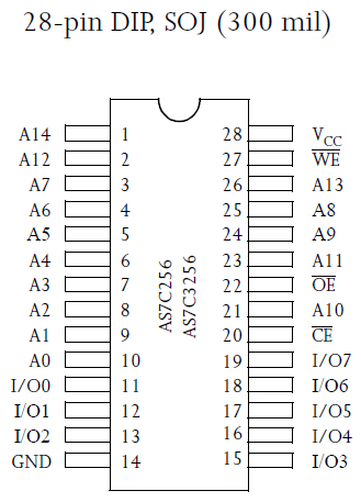
i've been getting interested in the actual design of an 8088 PC-like motherboard, and i've been toying around with schematics and connections and reading data sheets. i'm wondering something though. the DIR pin on the 74LS245 bus transceiver. this connects directly to the DT/R pinout on the 8284A bus controller, correct? which side on of 74LS245 should the 8088's data pins be connected to, bus A side or bus B side?

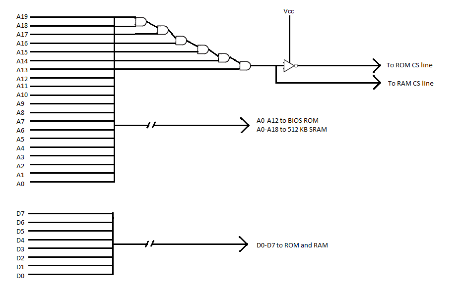
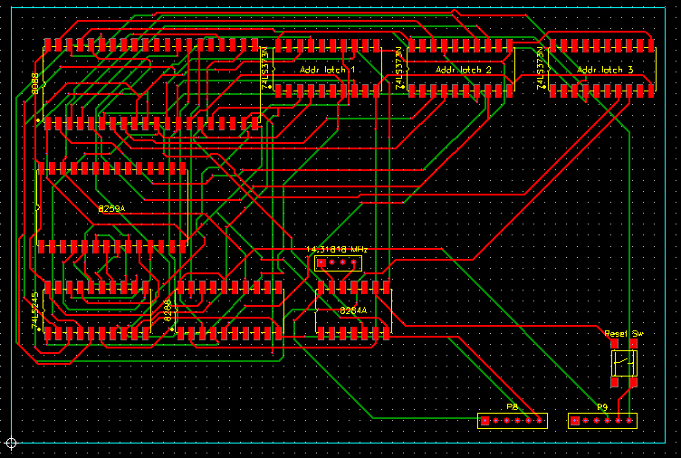
maybe i'm not understanding this right at all? pretty new to this sort of thing. so far i've come up with this...... sorry it's not very easily decipherable:

mobo1.png


if i'm way off base with the whole thing and i should give up, tell me now lol. :confused:
 
Last edited:
Hi! You might want to get in contact with Sergey since he is designing nearly the same thing. He is pretty far along in his design and probably would appreciate the company. I've seen photos of his prototype and it is quite impressive. I think he is on these forums or you can contact him on the N8VEM mailing list too.

Thanks and have a nice day!

Andrew Lynch

PS, what EDA software are you using? Switch to KiCAD while you still can!
 
i just looked up his project, wow his board plays games already. i'd probably just be bothering him with these trivial questions. ;)

as far as the software, i'm using pad2pad because you can place orders from right in the program and they'll solder on components as well. it's expensive though. i suppose i need to get myself a pretty large breadboard to play around with the design. i can't spend $150 and wait 2 weeks every time i think i need to modify something heh. i've got a radioshack one, but i doubt it'll be enough.
 
Bob Grossblatt's "The 8088 Project Book" (ISBN-10 0830631712) is highly recommended, and very humorous too...
 
i can't imagine this exists, but is there any electrical circuit simulation software similar to livewire that has pre-defined ICs such as 8088s and support chips? that would be a ridiculous feat of coding, if so..
 
There were a couple of DIY 8088 projects published in the early days of the IBM PC. Perhaps in Microcomputing? I'll have to look one up. ISTR that they skirted the problem of a video display and keyboard by providing RS232 I/O.

I think I even have schematics for one.
 
i was thinking of possibly using RS232, although it shouldn't be too difficult to wire a CGA card into it? keyboard gets a bit hairier, since there's a whole other IC that would be involved. if i actually build something, i might leave the DMA controller out just to keep it simple. i could mod the source code of the generic XT BIOS i used for my x86 emulator to bypass a lot of the checks that would halt the system and use that to POST.
 
i was thinking of possibly using RS232, although it shouldn't be too difficult to wire a CGA card into it? keyboard gets a bit hairier, since there's a whole other IC that would be involved. if i actually build something, i might leave the DMA controller out just to keep it simple. i could mod the source code of the generic XT BIOS i used for my x86 emulator to bypass a lot of the checks that would halt the system and use that to POST.

On the original 5150, the DMA controller was used not only for the floppy access, but more importantly as the DRAM refresh facility. There were specialized DRAM refresh controller chips, but they tended to cost almost as much as the 8237. If you go with static RAM, you can certainly get away without a DMA controller. Heaven knows, SRAM is much cheaper than it was when the PC came out.

I've got a DRAM card from one of those "DIY lookalikes". It's not only got the DRAM, but also the serial controller--an Intel 8274 MPSC.

If you're doing a minimalist-type of system, you may also want to consider using an Intel 80188 (you can get them with built-in serial ports) or better yet, a NEC V40 (comes not only with a serial port, but also DMA and interrupt controller. The V40 was used in a couple of PC-compatibles.
 
If you want to prototype yourself, I'd wire wrap the project. Wire wrap is my favorite method for prototyping high-IC-count digital circuits. The tools and wire are cheaply available...the only expensive part is the sockets, but you can hunt around for them. If you'd like a used wire wrap board with pre-inserted rows of pins (no sockets required), PM me as I have several (you'll have to cut/unwrap the old wires).

+1 for SRAM too...there's no real reason to go with DRAM with modern SRAM devices being so cheap. You can get a single-chip device that will satisfy the memory needs of your project, even if you don't use the device's entire capacity.

I'd also agree that switching to a different layout/CAD solution would be wise...I've heard good things about KiCAD, especially from Linux users. I personally use CadSoft EAGLE at the moment, because it was the best package that worked with Linux and had a free version at the time I started doing PCB layout. EAGLE is widely used by hobbyists (Make, Hackaday, et c.) who only need to make small boards, and I'd imagine your project is larger than EAGLE would be useful for.

If you just want a DIY x86 board to play with, check out John Coffman's SBC-188 project. I just ordered one of the boards + floppy controller from Andrew. They've got it booting DOS from floppy/CF card. I'm interested in possibly getting CP/M-86 running as well.
 
I've got a little box here, powered by a 12VAC wall wart. Its stated purpose is to sit between a printer and a printer port on a PC and connect to a telephone line. It's got a NEC V40 CPU, a 1.44MB floppy drive driven by a National DP8473 controller, a DS1215 "phantom" time chip (with a 1F cap to keep it going over short power outages--no battery), a Yamaha FAX DSP, a couple of 74LS374s for the printer port and 256K of DRAM. It's smaller in footprint than a 5.25" disk drive. All ICs are PLCC or DIP; i.e. through-hole. The code resides in a 128KB EPROM.

I have no use for it as its stated purpose, so I looked at it and discovered space for a 10 pin header, so I took a careful look and determined that it connected to the serial port on the V40. So I rigged up a small MAX232 board that provides RS232C signal levels and got to work.

I found it was pretty easy to write enough code to get a serial-port debug monitor going and added routines to access the floppy drive (same I/O ports as on a standard PC) and the clock chip.

And that's where it sits today--I suspect that one day I'll put CP/M-86 on it (DOS would be a waste, owing to PC incompatibilities such as having no video).

The whole point of this is that you should really look at the V40. You can get going with a functional design for far less effort and problems than if you were to use an 8088.
 
good info, guys. thanks. i think i'd rather use an 8088, chuck. makes it a bit more interesting to see how the different ICs interface.

i've got a question here, though. for memory, i plan to use a regular old 1 MB 30-pin SIPP (only hooking up A0-A18 for 512 KB) to simplify things.. but how am i supposed to handle the proper timing for DRAM refreshes, and what would i use to generate a RAS signal? i wonder if i have any SRAM laying around.. doubt it.
 
Your best source on timings is the datasheet on the SIPP/SIMM chips themselves. It can get to be pretty spooky at time. RAS/CAS timing was often generated with a delay line, although cheaper solutions are certainly possible. Basically, all you have to do is work out the basic read and write timings (note that DRAMs are all MOS, so that they can be a bit finicky with regards to layout and load capacitance). One of the 8237 channels can be set to perform auto-initializing DMA cycles, so you don't need to worry about the special refresh modes of the DRAM.

Personally, I'd stick with SRAM; you can get a 32-pin 512KB DIP for $8-10 and save your mind.
 
i gotta agree. i will definitely go with SRAM. and i realized that i actually have gobs of it available. it's time like these i'm glad i'm a hoarder that doesn't even trash dead motherboards. i have various toasted 386 and 486 boards with SRAM for cache!

got a 386 board here in front of me with four Alliance AS7C256-25PC chips. datasheet: http://www.datasheetcatalog.org/datasheet/AllianceSemiconductor/mXususx.pdf

looks like it's 512 KB.

The AS7C(3)256 is a 5V/3.3V high-performance CMOS 262,144-bit Static Random-Access Memory (SRAM) device organized as [size=+1]262,144 words × 16 bits[/size].

sram.png


EDIT: wait a sec, why does it only have A0-A14? that's 32 KB addressable.
 
Last edited:
i gotta agree. i will definitely go with SRAM. and i realized that i actually have gobs of it available. it's time like these i'm glad i'm a hoarder that doesn't even trash dead motherboards. i have various toasted 386 and 486 boards with SRAM for cache!

got a 386 board here in front of me with four Alliance AS7C256-25PC chips. datasheet: http://www.datasheetcatalog.org/datasheet/AllianceSemiconductor/mXususx.pdf

looks like it's 512 KB.


EDIT: wait a sec, why does it only have A0-A14? that's 32 KB addressable.

It's also 262,144 bits--also note that there are only 8 data lines. Here's the datasheet..

A Samsung KM684000 is a nice 32-pin through hole 5V 512Kx8 SRAM that's more than fast enough and $9.60 at Futurlec.

3.3V SRAMs in SMT are cheaper, but they're probably not worth the extra trouble.
 
ah, yeah. bits. should have been obvious. i've not got much experience with serious circuit design and datasheets, but i'm learning. the most complicated thing i've built is probably a little converter to connect my car's diagnostics connector to a laptop's serial port. thanks for the tip on that samsung part, it looks good. $10 is worth it to not have to mess with using hex inverters to make these 32 KB chips appear contiginous.

although, it would be fun to be able to say i built it using nothing but chips off of junk boards like it was some sort of unholy franken-PC. ;)
 
Last edited:
alright, so assuming that i use the 512 KB SRAM chip and an 8 KB BIOS ROM that i want to start at FE000h, does this (ghetto mspaint) schematic look like what i want to do? also, i think OE should stay tied low permanently?

memoryschem.png


this is fun.
 
visible results... LEDs on the addressing lines showing it cycling through F0000h to FFFFFh looking for code to run. :rockon:

 
Yes, but don't do it that way--you'll get a nasty/noisy edge on that A13-A19 AND--use something like a 74LS30 instead.

i've got a 74LS20P, a dual 4-input positive NAND on a dead mobo. looks perfect for the job. time to plug in the soldering iron!
 
Back
Top