• Please review our updated Terms and Rules here

XT-FDC project level of interest

$160 for 4 boards??? How big are they? How many layers? Sounds kinda steep...

Hi Mike
They are standard 2-layer PCBs from www.33each.com and are top-notch prototype boards. They are an excellent value and can be up to 60 square inches of any shape. Very nice and well worth it. I highly recommend them.

Thanks and have a nice day!

Andrew Lynch
 
For that shape and size 40 a pop is quite cheap for a proto.
If i am given a Gerber file i could mill it myself which would result in a lower quality proto board and i have to stamp the via's in by hand hence my comment to go easy on the via's.

So that would raise the total proto board to 5 Besides that i am sure Andrew still has a ace up his sleeve.
 
Given that this is all through-hole, it'd be simple enough to wire-wrap up a prototype. I realize that this isn't the way it's done today, but I still do mine that way.
 
Hi! Good news! Some additional prototype board donations came in and we are now up to $130! Woo Hoo! Almost there!

The current design has about 90 vias and 552 pads. If you are planning to hand drill and plug those vias it is going to be some serious work!

Chuck and I are still going back and forth on the design. The main issue remaining is what to do capture configuration information.

I think we are getting close though. More updates as they come available!

Thanks and have a nice day!

Andrew Lynch
 
Hi Mike
They are standard 2-layer PCBs from www.33each.com and are top-notch prototype boards. They are an excellent value and can be up to 60 square inches of any shape. Very nice and well worth it. I highly recommend them.

Andrew Lynch
Looks like you've pretty well covered it anyway.

But you might try this prototype service one day:
http://oshpark.com/pricing
3 copies of a half-length ISA board would cost abt. $75.00 incl. shipping; silk-screen & solder mask both sides, gold coated.
Larger quantities $1.00 per sq. inch
 
Hi
That's a neat idea but I wouldn't want to mess up the XT-IDE by combining it with a floppy controller. I guess I've adopted John Monahan's philosophy of one function per board. It makes for a much simpler design and a *lot* easier to debug. Also I think there would less interest in a combination board rather than a single function boards.

Thanks and have a nice day!

Andrew Lynch

Multifunction is the way to go once you get the single function card working correctly, you wouldn't want 5 computers performing single tasks would you?
 
Hey Andrew, it's possible to have an emergency boot disk image on ROM in this board? A backup free dos with minimal disk utility, with an option to boot using a menu like the one in XT-IDE, this would be very handy. I think there's space to do this with a 27512, and the costs won't be in sky, just an idea, of course.

Hi Lucas,
We've made some progress on the storing of configuration information on the XT-FDC design. We can put the information in the same EEPROM as the BIOS and it can be write protected to keep it from being overwritten. The good news about it is it frees up what used to be an input port for switches now can be reused as an output port for ROM upper address lines. I think it makes the larger ROM idea a lot more feasible and so I'd like to revisit this concept.

I'd suggest a dual memory approach. The BIOS and configuration information would be stored in a 28C64 with write protect. This is part of the design already and is required if you want to use the XT-FDC to boot using its BIOS. It is basically reused from the original XT-IDE design and pretty reliable. It is still "optional" if you don't care about the FDC BIOS or config information and just want FDC. It has to be simple, reliable and stay in memory at all times (no switching memory context with a latch or it will crash the CPU if running code in the BIOS ROM).

For the Flash ROM drive add the output port latch that is just a conversion of the switch input latch that is already there left over from the input switches. Add another memory decoder 74LS688 and a 29F040 Flash ROM for a 512KB "ROM drive". It would contain essentially a custom 512KB floppy disk image and could boot just like a floppy. Actually I think a raw image of a 360K floppy would work "as is" or nearly so assuming the FDC BIOS code is able make it look like a drive to the PC's main BIOS.

The key is being able to reuse/modify the IO port decoder circuitry for the latch. The PC8477B/DP8473 has a "hole" in its registers at 0x6 where we can fit in a IO port within the existing range of the FDC. Otherwise it would require its own duplicate IO port decoding logic *or* use twice the IO addresses for a single device. Once we have the latch available adding in the memory decoder and the Flash ROM use only a couple more components plus some passives.

I think it is an efficient design to just have a reliable permanently resident small ROM for BIOS/config and a separate Flash ROM for the data. Trying to use one chip for both would be complex because you'd have to keep at least one page of the Flash in memory at all times while trying to switch another page. It is possible but would require some complex glue logic and more parts. It requires only a few parts to just use a small BIOS ROM and a larger Flash memory as separate subsystems *and* it decouples the BIOS ROM from the Flash ROM which allows it to be an optional component -- potentially saving costs.

Tonight I will update the schematic and post it for review. Since the changes are relatively modest it should take only a few days to update the PCB layout and optimize the trace routing for a prototype board.

Thanks and have a nice day!

Andrew Lynch
 
Tonight I will update the schematic and post it for review. Since the changes are relatively modest it should take only a few days to update the PCB layout and optimize the trace routing for a prototype board.

Hello Andrew,
I look forward to the new schematic, the idea is awesome, thank you.

Lucas
 
lynchaj said:
... frees up what used to be an input port for switches now can ...
Bugger, I love me some switches, mostly because I have a tendancy on some machines to move a lot of bits around and reconfigure things (e.g. my 'drive-testing' 386).

It's not important but a couple of questions:

- would it be possible to allow the configuration for drives 0 and 1 to be controlled by the computer's BIOS at all? And let the controller configure drives 2 and 3 (if fitted)?
- would there be a 'press KEY to configure' on startup?

Just trying to picture ways I could quickly configure drives without having to boot in to an OS first (but at the end of the day its a 'nice to have' rather than a 'must have')
 
It's possible to boot from any drive without knowing the exact configuration. Similarly, it's possible to tell if a drive exists at a specific unit address without being explicitly told.

Right now, my plan is to be able to determine drive type on boot (Drive A: first request to read track 0, sector 0) even if not configured. That should be enough to get DOS up. You can then enter the configuration utility from DEBUG in the same manner that the hard-disk low-level format routine is invoked. Thus, there's no requirement for a separate utility, no annoying boot menus, and no switches.

At least that's the way my thinking is right now.
 
Looks like you've pretty well covered it anyway.

But you might try this prototype service one day:
http://oshpark.com/pricing
3 copies of a half-length ISA board would cost abt. $75.00 incl. shipping; silk-screen & solder mask both sides, gold coated.
Larger quantities $1.00 per sq. inch

Hi
The XT-FDC PCB is roughly 22 square inches. Your $75 quote would be a for 15 square inch PCB so scaling that up to XT-FDC means it would cost $110 for 3 PCBs which is in line with the Advanced Circuits www.33each.com pricing. If you compare apples-to-apples most prototype board houses cost about the same per board.

Thanks and have a nice day!

Andrew Lynch

PS, I updated the schematic and PCB layout on the wiki (see URL above). Everyone please review it and post any comments. I think this is the configuration we should take to prototype board once the trace routing is cleaned up. That should take a few days.
 
It's possible to boot from any drive without knowing the exact configuration. Similarly, it's possible to tell if a drive exists at a specific unit address without being explicitly told.

Right now, my plan is to be able to determine drive type on boot (Drive A: first request to read track 0, sector 0) even if not configured. That should be enough to get DOS up. You can then enter the configuration utility from DEBUG in the same manner that the hard-disk low-level format routine is invoked. Thus, there's no requirement for a separate utility, no annoying boot menus, and no switches.

At least that's the way my thinking is right now.

Hi Chuck
That makes sense to me. The primary function of the XT-FDC is to support floppy drives so that should be of paramount importance.

If/when others want to help pick up the BIOS source code and extend the functionality to include boot menus, storing configuration data, using the Flash ROM for booting, etc it should come later. The XT-IDE BIOS evolved a similar manner and there may need to be multiple versions of the BIOS depending on what builders want to do with it.

Thanks and have a nice day!

Andrew Lynch
 
Hi
UTSource.net and eBay are probably your best bet. Neither chip is very common but they are available.

Thanks and have a nice day!

Andrew Lynch
 
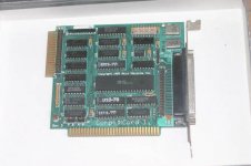
Maybe would be a good idea to have a slot connector side-by-side with P18? Like in this card:

floppy.jpg

I got an IBM floppy controller recently, and the cable didn't had that usual pin connection, only slot.
What you guys think?
 
Hi
Adding a 34 pin card edge connector is certainly possible although it does add cost in three ways. I can't tell you the exact amount but it would be more expensive that the XT-IDE since it would have a different planform PCB.

1. increases the rectangular square area of the PCB by a couple of inches (the PCB has to fit in a rectangle and that's how they calculate PCB area, not the actual PCB area itself and you don't get a discount for the material they trim off :-( )
2. gold fingers
3. slot cut into board at keying location

It can be done but it is pricey. Are the card edge connectors used enough to warrant the extra expense? I just converted my floppy cables by clamping on an IDC connector that way you can use either connector. Definitely something to consider though.

Thanks and have a nice day!

Andrew Lynch
 
Back
Top