• Please review our updated Terms and Rules here

Modern XT compatible PC on FPGA with real 8088

I entertain proofs or challenges to the above.

Looked at XT schematics - my brain can't comprehend the logic of READY circuit... At least I couldn't find any special WAIT signal for RAM, that does not exist for ROM.

One more thing, from Technical reference:

The ROM ... has an access time and a cycle time of 250-ns each.
The RAM ... an access time of 200-ns and a cycle time of 345-ns.

The clock period for XT is 210-ns, and 8088 requires at least 4 clocks for one instruction, so I don't see why 345-ns RAM cycle time can be critical and require extra wait states...
 
I entertain proofs or challenges to the above.

I challenge thee!

There must be some reason other than RAM/ROM why one was faster - looking at the XT schematic I don't see any mechanism by which RAM and ROM accesses could have different timings. Accessing a byte takes 4 cycles, and that's determined by the 8088. There is a line that ISA devices can use to insert wait states (the CGA card uses it) but none of the motherboard devices use it. Also there's nothing on the motherboard that can tell if an access from the 8088 is code or data (the 8088 pins that expose that information aren't connected to anything except the 8087 socket).

So perhaps the instruction encoding was slightly different in the RAM version of the routine you tried? Or perhaps word alignment is significant? (I don't think it is on 8088, but it's possible there may be remnants of 8086 and non-alignment delays in some parts of the 8088). Another possibility is that it depends on exactly where the CRTC is in its horizontal cycle when the routine starts (but if that were the case I would expect to sometimes see snow with the ROM routine).

Could you post the code you used to test this somewhere so I can try it for myself?
 
Could you post the code you used to test this somewhere so I can try it for myself?

It was scratch code, long gone, but all I did was copy the int 10h,ah=09 routine I found in ROM to plot a character+attr:

Code:
seg000:13E2 loc_13E2:                             
seg000:13E2                 in      al, dx
seg000:13E3                 test    al, 1
seg000:13E5                 jnz     short loc_13E2
seg000:13E7                 cli
seg000:13E8
seg000:13E8 loc_13E8:                             
seg000:13E8                 in      al, dx
seg000:13E9                 test    al, 1
seg000:13EB                 jz      short loc_13E8
seg000:13ED                 mov     ax, bx
seg000:13EF                 stosw
seg000:13F0                 sti

...to RAM, ran it there, and saw snow. Then, I replaced the MOV AX,BX with XCHG BX,AX and the snow was avoided. I believe I then did some REP LODSW tests using the zen timer from system RAM, video RAM, and ROM, and saw that the system RAM and ROM times were identical, which confused me.

I remain confused, although maybe the info newold86 posted above is relevant? Maybe the BUI can fetch from ROM quicker than RAM somehow?
 
Maybe the BUI can fetch from ROM quicker than RAM somehow?

That's not it - the BIU fetches code bytes in exactly the same way it fetches bytes for "REP LODSW".

That snippet gave me another idea about what the difference is, though - I wonder if interrupts are off going into the routine when it's running from ROM (via an INT 0x10 - the INT instruction disables interrupts) but on for the RAM routine. That would affect the set of character positions that the "stosw" can happen at, and possibly give the result you saw.
 
LEA performs the effective address calculation of the second argument and puts it into the first argument, but "DX" is not a valid EA expression, so what is this supposed to do? What does this do on a real 8088?

I couldn't stop thinking about this, so I had to test it. It appears to do the following:


  • Real 8088: AX = SP, flags unchanged
  • PCEM emulator: AX = Random value, flags unchanged
  • PCE emulator: Console window prints "undefined operation [8D c2]"; AX unchanged
  • PCjs emulator: Crashes; prints "Fatal error: Undefined opcode 0x8D at 0xnnnnnnn"
  • DOSBox: Crashes
  • VirtualBox: Crashes (or, prints an exception if running QEMM inside the VM and allows you to reboot)

Chuck, is AX = SP what you expect of 8Dh C2h?
 
LEA performs the effective address calculation of the second argument and puts it into the first argument, but "DX" is not a valid EA expression, so what is this supposed to do? What does this do on a real 8088?

I couldn't stop thinking about this, so I had to test it. It appears to do the following:


  • Real 8088: AX = SP, flags unchanged
  • PCEM emulator: AX = Random value, flags unchanged
  • PCE emulator: Console window prints "undefined operation [8D c2]"; AX unchanged
  • PCjs emulator: Crashes; prints "Fatal error: Undefined opcode 0x8D at 0xnnnnnnn"
  • DOSBox: Crashes
  • VirtualBox: Crashes (or, prints an exception if running QEMM inside the VM and allows you to reboot)

there is some discussion on this for the 8086 at http://www.os2museum.com/wp/undocumented-8086-opcodes/

Raúl Gutiérrez Sanz says:
April 12, 2014 at 7:55 pm

LEA AX,DX: As Joshua Rodd said, it loads AX with the last computed effective address. and I would add: Excluding addresses computed for flow control (addresses to be stored in IP).

LEA computes the memory address of the 2nd parameter and seems to store this address in an internal register before storing it in the 1st parameter. If the 2nd parameter is not in memory, no computation is done, and LEA seems to take the previous contents left in this internal register.

So, the general case is that LEA AX,DX after an instruction whose parameter is [1234h], will load 1234h in AX, regardless of DX.

After XLAT, it will load BX+AL.

After PUSH, PUSHF, POPF and CALL it will load the resulting SP. Presumably the same for INT, RET and IRET, but I had no time to test them.

After POP it will also load the resulting SP, except for POP [1234h] (it will load 1234h).

JMP will not alter the last computed address, except for JMP [1234h].

After LES and LDS, it will load the parameter address + 2. In the 8088 it could be different.

CMPSB and CMPSW seem to calculate the instruction of next elements after performing the comparison (to update SI and DI), and they update SI first and DI next. So, after those instructions, the updated DI will remain in the internal register.

Raúl Gutiérrez Sanz says:
April 19, 2014 at 12:32 pm

“After PUSH, PUSHF, POPF and CALL it will load the resulting SP. Presumably the same for INT, RET and IRET, but I had no time to test them.”

Confirmed, but one exception: After RET N, LEA AX,DX will load SP – N in AX (because RET N discards parameters, but does not access them).

It’s also worth noting that INT seems to PUSH the return address after reading the interrupt handler address from the vector table.
 
Happy to be corrected, thanks!

So, this is extremely interesting; 8D C2 can be used to load AX with a word value smaller than an actual MOV AX,immed. I can't immediately see a "win" for using it, but it's fun to think about.
 
I've viewed 8D C2 as a debug tool for determining the last calculated effective address. That is, when you have several paths to a single point, it can be difficult determining how you got there. A shame that there's no equivalent facility on the later x86 chips.

Most emulators will stumble on that one.
 
This is indeed a very interesting thread and project, newold86! (and of course also the 8D C2 discussion, however unrelated). Would you let us know how your project is developing?
 
This is indeed a very interesting thread and project, newold86! (and of course also the 8D C2 discussion, however unrelated). Would you let us know how your project is developing?

Unfortunately, almost abandoned the project - don't have enough time :(

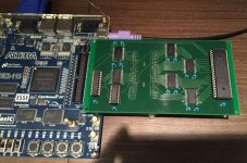
At the end, made improved board (plugs directly into FPGA board, removed a couple of IC's) - had some electrical noise issues previously, new board works without any problems.

xt2.jpg

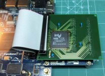
Also, started similar project with 486:

at1.jpg

The progress with this one was very modest - very basic operations (blinking LED), everything else postponed until have more time and interest...
 
I've viewed 8D C2 as a debug tool for determining the last calculated effective address. That is, when you have several paths to a single point, it can be difficult determining how you got there. A shame that there's no equivalent facility on the later x86 chips.

Most emulators will stumble on that one.

Tested this on various versions of 8088, 80C88, and V20. All 8088 and 80C88 indeed load the last calculated effective address to AX. On V20 situation is a little bit more interesting. Sequence like:

MOV BX,[address]
LEA AX,DX

will load to AX the address itself + the value stored at that address; in case of JMP [address] it will load just the address.
 
Not only that, but Intel boxed themselves into a 1MB address space, which was incredibly short-sighted.

And here is what 8086 designers have to say (on page 17):


Various alternatives for extending the 8080 address space were considered. One such alternative consisted of appending 8 rather than 4 low-order zero bits to the contents of a segment register, thereby providing a 24-bit physical address capable of addressing up to 16 megabytes of memory. This was rejected for the following reasons:

Segments would be forced to start on 256-byte boundaries, resulting in excessive memory fragmentation.

The 4 additional pins that would he required on the chip were not available.

It was felt that a 1-megabyte address space was sufficient.
 
Segments would be forced to start on 256-byte boundaries, resulting in excessive memory fragmentation.

The 4 additional pins that would he required on the chip were not available.

It was felt that a 1-megabyte address space was sufficient.

Silly. There were certainly 44 pin DIPs around. I don't get the issue about 256 segment boundaries--calulation of segment addresses from offsets would have been much easier. "Sufficient" is just a bit of short-sightedness.

I attribute the whole thing to be that Intel wasn't really serious about the 8086 as a long-term project. As I recall, the Big Thing intended for Serious Work was tha 432--which, as we know, soon took over the world of computing...
 
I have a book, circa 1982, that touts how iAPX432 will take over the world.

Well, its successor the i960 did take over... a small part of it. Very small.

It is lucky for all of us that Intel's 432 processor project never made it back in the early eighties. Otherwise a really horrible Intel architecture might have taken over the world. Whew!

-- Steve Friedl
 
Last edited:
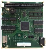
Decided to move on with my projects a bit more... Finally found enough time to get running something that started quite some time ago:

_IMG_0902.jpg

The idea is to create 100% hardware accurate replica of original PC XT (plus A LOT of other features, of course), but with all "small" chips inside of FPGA.
Current project is the "proof of concept" - to test certain things I wasn't sure about. Possibly, if I have time and desire, I make "release" version of the project...

Still doing a lot of troubleshooting to find out why some extension cards/software don't work together well, but it's coming there (hope so :)... At least, yesterday managed to troubleshoot last (hopefully) big issue - DMA sometimes would freeze the board, so now SoundBlaster is producing beautiful noises :)

Unfortunately, my reflow oven is too small, so I couldn't put more than one ISA slot on the board - struggling now :(

Also, FPGA doesn't have enough pins for all my ideas - will need to use BGA package next time, with many more pins...
 
Very cool!

I can't see the pinout on the video header; I'm assuming it's VGA?

Yes. Lack of FPGA pins didn't allow me to install TV/CGA/EGA connectors as well :(
Of course, you can use any video card in the slot, but I wanted to have something on the board also...
 
By the way, does anyone know some game that works on CGA but supports SB ? Really need it for testing purposes...
 
Back
Top