• Please review our updated Terms and Rules here

Build your own PDP 8I, Part 3..

Hi All;

I have not wired all of the individual Led's, but I am combining that with finding mistakes and such, as I go..
I have found two mistakes already, one was a not clearly labeled signal and so I had it on MIC.L and it needed to be on MIC.H..
I think the other was clearly a late night too tired to correctly wire, mistake..
I am now going to check the Mux M signals, Mux Mb signals and the Mux Accumulator signals..
As they all show a similar pattern..
I am having to make another change, for my sanity and not that the system needs the change..
For the first 4 IR's (IR00-IR03), I need to change what the Led's show, in normal mode they would show true IR00-IR03, but in other mode it would show IR04 + MA00-MA03..

THANK YOU Marty
 
Last edited:
Hi All;

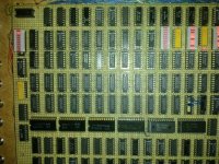
I have all of the individual LED's wired up..
So I can attach the wiring for the switches and
then I can mount the the Board in it's vertical position if needed.. But, most likely I will lay it down while making an attempt at debugging the Board..
As I wire in each Load Switch, I check it for workability, and I am finding mistakes and mis-wirings..
I have done the LDAC, LDIR and now LDPC,, where there is a wiring error.. A pin that should have no wire on it, has a wire on it..
I found the problem, It was one of those sockets that originally was for a 16 Pin Ic and the sticker on the back of it is still numbered as a 16 pin IC, but, I had to put a 14 pin IC (74LS10) there in its place.. And so the mixup, but the PC Load works fine..

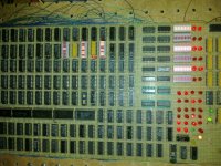
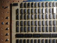
001.jpg 002.jpg

THANK YOU Marty
 
Last edited:
Hi All;

Al, Thank You for Your question..
"" Where are the bypass caps? ""
Where they would go has been wired in.. I Just haven't put them in, Yet..
I have some, at this point I don't know how many..
Since I am running at such a low frequency and I wanted to get the main wiring done, then I would put them in..
I just haven't put them in..
On a side note, I do have the switches on the right hand side wired in and working..
Just for You Al, I put some in.. I will have to get about 150 at J. B. Saunders here in town, when I get by there..

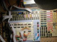
003.jpg

THANK YOU Marty
 
Last edited:
Hi All;

I am going to next wire in the Data switches, and after that the circuit for Single Stepping..
All of the Data lines are wired in.. But, there is a problem..
So, I will need to wire in the Single Step Circuit for sure..
The Single Step Circuit is wired in now..
Then we will see what works and what doesn't work..
I found another goof up, for some unknown reason, I wired in MB00-MB03 completely, but I didn't wire in MB04-MB11 to the Registers themselves..
That made things alot better, still not perfect..
I have found six things that I need to change, that are different than Dave's Schematic.. Mostly, things like a CPx wrong polarity, and OPGx wrong polarity..
All of that is fixed, and things work better..

BUT, there is another problem, when the MA(L) is pressed, the MA Register won't show the result..
I have chased the signal all the way thru the MA(L), which is there.. The MA Register is showing that it is getting the input and there is a Clock signal.. I've changed all of the IC's having anything to do with this Register.. Including the Register itself..
But, to no avail..

THANK YOU Marty
 
Last edited:
Marty,

Yes - the polarity of the CPx and OPGx kept me amused for a while - stick with what I have used (that seems to work)...

Is it just MA(L) and the MA register which is a problem or does it work OK (for instance) with IR(L)?

Don't forget the IR register has the 74174 /CLR pin (pin 1) tied 'high' (unused) whereas the on the MA register it is connected to A0 from the fetch state machine. If A0 goes LOW it resets the MA register. Could this be your problem and not the MA(L) signal and/or the MA register itself?

Dave
 
Hi All;

Dave, Thank You for Your reply and suggestions..

"" Yes - the polarity of the CPx and OPGx kept me amused for a while - stick with what I have used (that seems to work)... ""
I have been going back to Your Drawings, multiple times and that is/was How I found out what some of the problems were..
"" kept me amused for a while "" Do You get amused easily ??

"" Is it just MA(L) and the MA register which is a problem or does it work OK (for instance) with IR(L)? ""
Actually, all that I am trying to do, is set each bit individually, in each register.. I haven't tried to see if it will copy the IR(L)..
Also, I am going to do a Clear on the rest of the registers, soon..

"" Don't forget the IR register has the 74174 /CLR pin (pin 1) tied 'high' (unused) whereas the on the MA register it is connected to A0 from the fetch state machine. If A0 goes LOW it resets the MA register. Could this be your problem and not the MA(L) signal and/or the MA register itself?
I didn't catch that, I will see if I have that wired up, or wired up correctly.. I don't think I ever noticed that and it isn't wired that way in this version, but it will be soon.. Good Suggestion.. It is done and wired in..

Things were working Yesterday fairly well, and Today nothing seems to work, It's probably something small, like a bent pin that is shorting something together, that was not meant to be..
At first there was no Clrx signal getting through, I changed the circuit and made it work, then also, there was No CPx's at all, when I would press a Button.. It still has that problem..
I can get it to count, but, I have to switch 6 and 7 or 2 and 3 or 1 and 5.. But it won't stop counting, then..
It looks like, once or if I can get this circuit or one like it to work, everything else register wise will work..

Dave, I have as You can see both L8 and L9 on ProtoBoard, so I can make any changes that are needed..

001.jpg

And on another side note, I have used up almost all of the 600 feet of wire of the primary three rolls that I bought, when starting this project.. I think I have about 20-25 feet left..

THANK YOU Marty
 
Last edited:
Hi All;

I am going to do an Ohm (connectivity) test of everything associated with page LD-9, especially L8, L9 and L10..
I've checked L7 and L8 along with the Muxes and I am going to check L5 and L6.. OK, they have been checked..

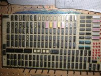
001.jpg 002.jpg

Everything checks out OK on those pages..
I put all of the Ic's back in and re-checked it, it still doesn't work..
I have ordered, just in case some 74LS42's, 74LS109's, 74LS163's, they should be here in about a week..
Something that I discovered by accident, is If I hold down the Clr Button, then it will Count, If I release that Button it stops counting, and also A4 will will turn off at CP0..
I need to figure out what all of this means..

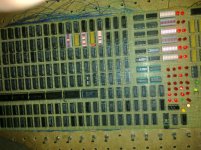
This picture is actually takes after the next posting, But, as there is not room for one more, I will put it here..
It shows the new 10 (8) position Bar Led to show Instruction status, such as AND, TAD, ISZ, etc..

009.jpg

Which shows that when the Clr is pressed, that an AND Instruction is issued..

I have a Dead short, I found out about it when turning the board over after doing some wiring..
One was a bent pin, I haven't anything other, but the short is still there..
I Found it, a new ++5 volt wire I had wrapped, had a bit of a longer tail than I had realized..

THANK YOU Marty
 
Last edited:
Marty,

Are you SURE you have L9 (exec f/f) pin 6 wired to L10 pin 1?

If you hold down CLEAR then the clear pin (pin 1) of L9 (exec) should go low which should reset pin 6 and set pin 7. Since pin 6 is now a zero - this should reset the 74163 counter (L10). I suspect your flip flop is 'round the wrong way' - or your clear signal is the wrong sense.

Pin 1 of L9 should go LOW when you CLEAR the PDP (i.e. it kills the EXEC signal). The same clear signal should also 'kill' the other half of the package - the RUN flip-flop.

Incidentally A4 doesn't turn off at CP0 - it is the other way round (cause and effect). When A4 is activated (goes low) this signals the 'end' of the FETCH cycle and that the EXECUTE cycle should start. M16 pin 8 is named GTE (Go To Execute). This signal resets the FETCH flip/flop and sets the EXECUTE flip flop. When the FETCH flip flop is reset it kills all the F and A outputs (as the fetch cycle is now complete) and starts the EXECUTE cycle. This starts by the EXEC flip/flop enabling L11 which produces the first clock (CP0).

So, A4 - triggers CP0 by causing a transition from the FETCH phase to the EXECUTE phase and not the other way around.

I really must get around to describing how the state machine works for you. I should be finished with my 'rush job' at work shortly so I may have a bit of time next weekend to describe it more fully.

Dave
 
Hi All;

Dave, Thank You for Your Helpful Reply.. I still have some other things to get done, But after that I will Check and Digest, what You have Stated.. And I will check Things a fourth time.. But, I also, will check that each Flip-flop is doing as You Described..

OK, I'm back..
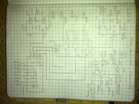
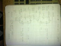
First to make sure we are working from the same Page.. Here are some pictures of the Relevant pages..
004.jpg 005.jpg 006.jpg

007.jpg 008.jpg


"" Are you SURE you have L9 (exec f/f) pin 6 wired to L10 pin 1? "" YES !!

"" If you hold down CLEAR then the clear pin (pin 1) of L9 (exec) should go low which should reset pin 6 and set pin 7. Since pin 6 is now a zero - this should reset the 74163 counter (L10). I suspect your flip flop is 'round the wrong way' - or your clear signal is the wrong sense. ""
I will Check !!!

"" Incidentally A4 doesn't turn off at CP0 - it is the other way round (cause and effect). When A4 is activated (goes low) this signals the 'end' of the FETCH cycle and that the EXECUTE cycle should start. M16 pin 8 is named GTE (Go To Execute). This signal resets the FETCH flip/flop and sets the EXECUTE flip flop. When the FETCH flip flop is reset it kills all the F and A outputs (as the fetch cycle is now complete) and starts the EXECUTE cycle. This starts by the EXEC flip/flop enabling L11 which produces the first clock (CP0).

So, A4 - triggers CP0 by causing a transition from the FETCH phase to the EXECUTE phase and not the other way around. ""
With a Led's as used to tell what is happening, I didn't know which was first.. But, I need to digest this Paragraph..

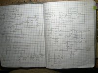
I am copying Your Answer above, to my Notebook, where I can read it slowly and Digest it and check out what You suggest..

"" I really must get around to describing how the state machine works for you. I should be finished with my 'rush job' at work shortly so I may have a bit of time next weekend to describe it more fully. ""
No Problem..
Please, check the Pictures of the Schematics, and make sure we are talking about the same thing..
In Your schematic from the program, (not Your Fault), but it shows the pinouts for like a 74163 Ic, in enough detail to show who connects to whom..
But, with the 74109's it shows a small square, and it is hard to tell who connects to what..

I am done copying it..
Dave, You make it look so simple when You explain things, but when I look at it, it looks like gobbledygook to me when I look at it..
Your description, already helped.. more in a moment..
"" or your clear signal is the wrong sense. ""
Yes, that was it, along with the Contrl signal.. When I had re-implemented the circuit, I thought that Clr.L meant that it was Low, But, what it really meant was it would be Low when the Button is pushed.. And so I had added another stage of invert to the signals..

I can set each bit in each register, but when I put a 7010 Rotate into the Instruction Register, it does not rotate the Accumulator, but it copies 010 into the PC register and possibly into the MA register, but that may be because of it being copied into the PC Register..
So, I need to find out about that..
Another Next problem, when I do a multiple Deposit, the MA Register does Not count up by One..
THANK YOU Marty
 
Last edited:
Hi All;

I decided that the last posting was long enough..
On the RAR instruction, when I put it into the instruction Register, and set a Bit in the Accumulator, here are the following steps, it seems to take..

State 0: I can't see any difference.. According to the Led's it looks for input
State 1: It copies the contents of the Accumulator into the MA Register.. MIC instruction comes on..
State 2: The first three Bits (the 7) of the instruction 7010 disappear from the instruction Register.. AND instruction comes on..
State 3: The PC Register is incremented..
State 4: The bit that is still in the Instruction Register is copied into the MA Register..
It then goes through the CP cycles.. At CP1 it Clears the Accumulator.. Then nothing else that I can see for the rest of the CP cycles..

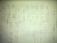
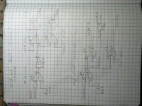
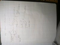
Here are some Schematic changes that I made for the Clr/Cont circuit, in the following pictures.. These work in my system..

010.jpg 011.jpg

I decided to change the OPGx circuit, back to what is originally there, and I think since it is late and I am tired, things don't work after doing the change..
I did this because of the State sequence above, and my having trouble with some 7432's in the circuit, or so it seems..
So, Monday, I will check to see if I did the wiring correctly, and that all of the OPGx signals are going to the proper place.. It will not show or deposit any bit to any of the registers, only '0000 ..

THANK YOU Marty
 
Last edited:
Marty,

About post #90

Yep - we are both talking about the same schematics...

As to why some of the parts in the schematics look physically like the chips and some look like the gates themselves - it is just what is easiest to some extent. Where a single chip is used as a separate entity (e.g. the SN74163) I have tended to use the 'chip view'. However, where devices contain multiple separate gates - it is easier to use the generic parts that come with the drawing package. For example, an SN7400 is a quad 2-input NAND gate. If three of the NAND gates are used in one part of the schematic and the fourth is used elsewhere - it would be silly to have some long snaking wires from one part of the schematic to some other unrelated part. It is also easier to use the LOGISIM generic part - as you just identify it is a NAND gate and specify whether it has 2, 3, 4, 8 or whatever inputs rather than have to develop a library for each different type of package. This is also one reason why I have buried the 'registers' within a drawing macro. I have used a standard SN74174 package and and 'wired' three of them together to make a standard 12-bit register. I have then used the register as a schematic symbol - with the data in and data out as 12-bit busses - this keeps the schematic more tidy and at the 'functional' level rather than a 'rats nest' of wires. Unfortunately, this means that the schematic can't be used easily to go to the physical implementation. Just one of the trade-offs in life I am afraid.

All of the control 'buttons' appear to be active low - i.e. when the button is not activated (e.g. DEPOSIT is not pressed) the signal is high. When the button is activated - the signal goes low.

Your 'multiple deposit' issue I had myself! Your 'friend' here are the tables on pages 104 and 105 of the Lab Manual. If you look on page 105 - you will see two columns, one headed DEP and the other EX. These are the EXECUTE clock pulses for these two 'pseudo instructions'. In CP6 you will notice the text "MUX = MA; ALU = A+1; MA(L);". This means when a DEPOSIT or EXAMINE is being executed - select the MA register via the MUX, set the ALU up to add 1 to the 'A port', and store the ALU result in the MA register. Now look at the schematic for LD15 in calculating MA(L). You will find pin 2 of E1 is wired to (DEP+EX)*CP6. This actually comes from M11 pin 8 on schematic LD13 (but it is not shown as such). The input to M11 pin 9 is (DEP+EX) which is also not shown anywhere - this actually comes from M8 pin 8 (schematic LD8). A slight 'niggle' - the ALU doesn't have an A+1 option, it is A+CarryIn (hence why M11 pin 8 is used to drive the CarryIn (CIN) logic on schematic LD 13). Phew!

About Post #91

I am a little concerned that an instruction of 7010 clears the accumulator? Look at the table on page 104 of the LAB manual under the column headed OPG1. The accumulator should ONLY be cleared at CP0 if IR4 is SET. 7010 has IR4 cleared - so there is something wrong here for sure!

You also say that at State 1 (I assume FETCH) that the ACCUMULATOR is transferred into MA? The PC should have been transferred into MA at this time in readiness for reading the instruction from memory into the IR register. One possibility is that the inputs to the ALU are reversed and the ACCUMULATOR and MUX bus lines are wired to the wrong 'ports' of the ALU. I wouldn't start messing with these wires though until you are 99.9% sure this is the problem! The other possibility is that some of the signals are inverted again. I found a lot of the CPx (and other signals) to be the wrong 'sense' on the schematic and I had to work them out for myself. Check your CPx signals with mine to see if we agree on the active high or active low sense.

The other thing I would strongly advise is to prove the 'architecture' logic first (the registers, MUX and ALU) and ignore all the control logic for now. if you don't get the architecture logic right now - you will never know where the problem is for sure. You should then 'expand' the logic by encompassing more of it - but in a controlled manner - checking (as far as you can) as you go. Once you have got something to work reliably - you can move on - safe in the knowledge that the most likely area where the next problem lies is the bit of additional logic you have added. This was the way I worked with my LOGISIM implementation.

To do this - remove all the chips driving the 'architecture' logic and force inputs to this manually from your breadboard.

If you look at drawing LD1 you will see the basic architecture consisting of the main registers (AC, SR, MA, M, MB, EA, PC and INPUT), the giant MUX and the ALU. First of all I would select the SWITCH REGISTER through the MUX to the A input of the ALU by setting the three bits (B4, B2 and B1) controlling the MUX to 5 (binary 101). What is present on the SWITCH REGISTER should now appear out of the MUX. Does this work?

Next, look at the data sheet for the 74181 under the table for ACTIVE HIGH DATA (Table 2). Setting the M input = 1 selects the LOGIC FUNCTIONS (this takes the carry in signal out of the equation). The MUX is wired to the A input of the ALU - so we want to set the ALU function to F=A (which is S3,S2,S1,S0 = 1,1,1,1). What enters the ALU port 'A' (which is the output of the MUX which is the SWITCH register from before) will now appear as the input to the bank of registers.

By setting up values on the switch register - they should appear at the inputs of all of the registers so you should be able to operate (say) the MA(L) signal manually and the value set on the switches should be written into the MA register. You should be able to do this for all of the registers - with the exception of the EA register (which is a logical expression) and the AC register (which contains a few extra signals you have to manipulate - set ALU = parallel load should be all that is required). I can walk you through this if you want.

After setting a different value into most of the registers via the technique above - you can then vary the MUX selector bits (B4, B2 and B1) to see if what comes out of the MUX (which should also be the same as what comes out of the ALU) is what you expect when you select the different registers (e.g. 0 = 000 = PC, 1 = 001 = MB, 2 = 010 = MA and so forth).

After that, you can start looking to see if the ALU is behaving properly by modifying S3..S0. For example, 1111 sets the ALU output (F) = the A input whilst 0000 sets the ALU output (F) = the NOT of the A input. 0011 set F=0.

If you can write a value to AC - then you can try the logical functions of the ALU by (for example) setting S3..S0 to 1110 means set F = A OR B (where F is the ALU output, A is the MUX input - set the MUX to the switch register to make your life easy - and B is the value in the ACCUMULATOR). S3..S0 = 1011 means set F = A AND B.

If things are OK at this stage, you can set M = LOW and try the arithmetic functions (you will now have to manipulate CIN as well).

Only when you fully know that this lot is working should you move on to the actual control logic. If you can't get this lot working reliably - then debugging the control logic will be virtually impossible because the control logic will be driving something that you are using to identify whether something is working or not - which is (in turn) faulty!

Dave
 
What Dave said in post #92.

"If you can't get this lot working reliably - then debugging the control logic will be virtually impossible because the control logic will be driving something that you are using to identify whether something is working or not - which is (in turn) faulty!"

Yep squared and cubed!

Take a look at Modem7's PC page. Particularly at his minimum diagnostic configuration. Absorb WHY this is important. Simply put, fewer parts being tested goes directly to fewer potential bugs affecting your tests. Use some of your LEDs, switches and flip flops to come up with a working "most general case" register. Should be a piece of cake to get it to do what you want per your understanding of what the design is supposed to do. Do something similar for the ALU. And for the MUX. Next you should be able to hook up some input switches and use them to pass information in a controlled & correct fashion from one already proven building block to another. After you know for sure that a given control signal should be in a particular state to make a particular event happen, you can take that particular switch out of the circuit and try to make the same thing happen with the control logic. Divide and conquer. One sub circuit at a time. One bug cleared at a time. If you don't understand how or why a particular part of the schematic is the way it is (and for me that's most of it), breadboard it and poke it in the guts until you do. Half of the fun (at least) of playing with these antiques is getting the sick ones fixed and learning in the process.
 
Hi All;

Dave and DDS, Thank You for Your toombs of information..

"" As to why some of the parts in the schematics look physically like the chips and some look like the gates themselves. ""
I was mainly looking at the 74109's and not being able to tell what wire went to what pin..

"" Your 'multiple deposit' issue I had myself! ""
I will look at the information You put on the screen and try to digest it, and Copy that whole posting to my notebook.. Ah, My sore hand..

"" Check your CPx signals with mine to see if we agree on the active high or active low sense. ""
I will check them again and put then in a list, just like I did for the OPgx tables.. Which is what I am going to check first thing Monday Morning..

"" The other thing I would strongly advise is to prove the 'architecture' logic first (the registers, MUX and ALU) and ignore all the control logic for now. if you don't get the architecture logic right now - you will never know where the problem is for sure. You should then 'expand' the logic by encompassing more of it - but in a controlled manner. ""
If, after doing the above, I cannot find the problem, then for sure I will do this, next..

"" By setting up values on the switch register. "" I sort of did this before, by setting each Register and each bit to that Register, I have to get it back to being able to do this.. Like it did Earlier Yesterday..

"" Only when you fully know that this lot is working should you move on to the actual control logic. If you can't get this lot working reliably - then debugging the control logic will be virtually impossible because the control logic will be driving something that you are using to identify whether something is working or not - which is (in turn) faulty! ""
I UnderStand, and Whether I like it or not, I need to take the Time to DO everything that You have described above for me to do.. I know I am in toooo much of a Hurry and just want it to work.. And NOT taking the time to both Understand it and to make sure it it right..

"" Take a look at Modem7's PC page. ""
Where is this ??

"" Divide and conquer. One sub circuit at a time. One bug cleared at a time. If you don't understand how or why a particular part of the schematic is the way it is (and for me that's most of it), breadboard it and poke it in the guts until you do. Half of the fun (at least) of playing with these antiques is getting the sick ones fixed and learning in the process. ""
Will do, and take to heart.. Thank You for this suggestion..
One of the Reasons, I used machine Sockets and Wire-Wrapped is that I can Pull every IC out and only leave in what is needed, and/or what is to be checked or adapted to Plug Board work..

THANK YOU Marty
 
"" Take a look at Modem7's PC page. ""
Where is this ??

Modem7 is one of the senior members here that hangs out mostly on the PC thread. His website is www.minuszerodegrees.com. For each of the early IBM 51xx machines he has a really detailed "how to" section including a "minimum diagnostic configuration" section. I wanted you to consider that line of attack, not so much the exact content of his site. If you connected the main chips for your ALU to a bread board, added some manual switches controlling the inputs you wished to investigate and some LED's that told you what the ALU was doing as a result you would have created a "minimum diagnostic configuration". Then you could say "If I put this combination of inputs on the ALU the outputs are supposed to do this". You'll have a hand full of hardware to breadboard and investigate instead of 100+ IC's and 600 feet or wire. Investigate and debug each possible set of inputs. When you're satisfied the ALU is working as a unit, do the same for the MUX, then each of the registers. THEN you can start tying those proven and somewhat more understood blocks together. The ALU is supposed to get its inputs from registers (or memory), do something to them and put correct outputs in a register or memory. So add some registers to your debugged ALU and test that out. You can work your way step by step, functional block by functional block, through most if not all of the design. Each time you can sort of depend on your configuration from the previous step, and focus on finding bugs in the part you just added.
 
Hi All;

DDS, Thank You for the link and the information.. And Your explanation of the process..

"" You'll have a hand full of hardware to breadboard and investigate instead of 100+ IC's and 600 feet or wire. ""
I understand Your approach, and It basically makes sense..

"" Each time you can sort of depend on your configuration from the previous step, and focus on finding bugs in the part you just added. ""
That makes sense to me, I can do it, with what I have.. Remember, I can take out every IC, and only plug in the ones that I need.. I sort of tried this when I first started to re-wire this 2nd version, and I found out that I needed most of the system to be there to test even a little bit of it.. And, so, I decided to go ahead and wire up the whole thing, since I could pull anything out that I don't need for a particular test..

But, I could not do it in/on a Breadboard, I find that too confusing even with three Ic's, not to say anything about a whole handful of Ic's, too many wires hanging all over the place and trying to make sure everything is hooked up..
I am used to the wire-wrapping and I can work with that, using Your approach, I can do the same..
Only, I don't have to wire some of it try the tests and take it all apart, and do the next application and test it and take it apart, and would still have to wire-wrap it up after the test is done..

I have and will though do small circuits, that fit into the problem at hand.. I have done it in the past, I can't right now think of an example, but I have done it..
One of the Tests that I plan on doing, as suggested by You and Dave is to set it up to do a Binary Count using one of the Registers and the 74181's to make sure that they are hooked up (wired) correctly and that it will count from '0000 to '7777 and the Link bit.. Along with the appropriate Led's for showing the count..

THANK YOU Marty
 
Last edited:
Hi All;

I Found the One wire that was Not wired correctly, and caused the problem, the wire for E13, pin 4 was accidently wired for OPG1.L instead of OPG1.H.. So, now that works correctly, like it did on Saturday..
Now I need to Read Dave's Tomb and work through each Paragraph, and Make sure that everything is correct and wired as His Schematic shows.. Will Post more as I find things, correct or not correct..
I have checked the Cin circuit against Dave's schematic and Both are the same, next is check that it is wired correctly..
Cin checks out OK..
After that, I will do as Dave suggested and check to make sure that all of the Cp0 signals are the same as His Schematic..
As Part of checking out Cp0.x, I have checked out the MUX control signals (B4, B2, B1) and the ALU control signals S0, S1, S2, S3 and M, Cin has already been checked against Dave's Schematic and all are OK Schematic wise..
I am going to check out that all are wired correctly..
I found, a Big Mistake, E14, pins 1 and 2, Pin 1, I think had been wrong in the schematic, which was fixed, before per Dave's Drawings, But, the wiring had NOT been changed.. So it was wired as OPG2.L instead of OPG2.H.. I fixed that..
Also, pin 2 had not been wired in at all, to Cp2.H, which is now done..
This would affect both B1 and B4.. B1, B2 has now been check and it is wired correctly..
And I haven't even finished doing the checking..
B1 had a Major Mistake, M14 pins 6 and 8 were Not connected at all to H1.11.. I have fixed this..
So, B4 is now wired correctly and checked..
This should Help things as well..
There is more to check, but it is somewhat better, still doing strange things, but better..
When putting a RAR at Memory Location '0000 and Jmp at Location '0001.. And doing a Continue, it does better than before..
But, still very strange, instead of Rotating the Accumulator, it counts the PC, which I think is correct, it also Writes to the Instruction Register bits 04-11, the inverse of the PC, and the same bits 04-11 are written to the MB Register, but not inversed..
And the Accumulator doesn't move, the bit in it that is set stays the same..
So more to check, I will next do the ALU Control signals, as stated before, and then check the rest of the CPx signals as stated earlier..
The ALU Control Signals are all correct, they and the MUX Control signals have been, Both check Dave's Documentation and for wiring..
I suspect one or more of the CPx's is in the wrong polarity, on something that I haven't checked.. But at least the ALU and the MUX's are Ok as far as the CP's and OPG's are concerned..

I made a List of all of the Cpx.L and Cpx.H signals, And the OPG's as well and so each one will need to be re-checked against His Drawings..
Then as DDS and Dave suggested, I will check the Muxes for correctness..

DDS, I have Not forgotten what You have said..

THANK YOU Marty
 
Last edited:
Hi All;

I have checked as far as Dave's Diagrams, my Schematic against His Schematic, for the following PC(L), IR(L), MA(L) and MB(L), and what I have agree's with what He shows..
I still need to check the wiring on these items and see if it is correct..

But, I do not have one item, in the PC(L) that He has, as it has to do with I/O.. But, I will implement part of it..
At present I have E13 connected to G16, without anything in between.. He has G18 and E17, between those points.. Only I will not be wiring IOS into the Mix, only IOT.H.. I for now will connect IOT.H to both Pins, instead of IOS to one pin and IOT to the other pin..

I have check with Dave's Schematic the following RAR, RAL, CLL, CLA and CML circuits.. The CLA circuit has a Problem/Mistake K4 pins 11, 12 and 13.. In my Old schematic it shows a 7400 NAND gate, along with my New Schematic,
But, Dave's Schematic has a 7402 NOR gate, instead of the NAND gate..
The NOR (7402) seems to be the proper gate, the CLA will pass the CLR Button , being pushed, and would not do so before..
The DCA to G2 pin 9 was not wired, I fixed this..
Also, found that none of the MA signals to the IR4.MA0-4 have been wired in as well..
All of the above need to be checked for wiring correctness, they have only been checked against Dave's Schematics..
I have checked the wiring for PC(L), MA(L), MB(L), and IR(L), as well as RAR, RAL, CLL, CLA and CML..
All of the OPG1 and OPG2 signals have been checked, as well as CP0.L.. The rest of the Cpx signals need to be verified and checked..

THANK YOU Marty
 
Last edited:
Hi All;

All of CP0 has been checked..
Next I am going through the rest of the CPx series..
All of the CPx have been checked..
Next is the Acc and Link circuitry to check.. OK, they have been checked out, both schematic and wiring wise..
Then I will work on different commands working on and with the accumulator.. Pulling out the necessary IC's So I can make it happen and working backwards from the Accumulator to its associated circuits.. Checking things as I go along..

THANK YOU Marty
 
Last edited:
Hi All;

Daver2, where in the Logisim Schematic Drawings, do You have the Logic for the IR04 and the MA00-04 ??
I Found it, You have a MUX where as the original has an 7400 (NAND) followed by a 7404 (Inverter), I have a 7408 (AND), And so I need to either use a 5 gate MUX which doesn't exist, or use two 74157's, which I don't have room for on the Board..
This could explains some of the problems, it has been having..
But, the circuit I have should work, doing the same thing..

THANK YOU Marty
 
Last edited:
Back
Top