• Please review our updated Terms and Rules here

Build your own PDP 8I, Part 3..

Marty and DDS,

PM sent to each of you with Version 0.2 of my LOGISIM simulation of the PDP-8 LD12 attached (a work in progress!).

Regards,

Dave

Thanks, Dave. Hopefully I'll have some time soon to really dig into this. Marty's project is certainly getting interesting.
 
Hi All;

DDS, Thank You, for saying that This project is getting interesting..
Right now while I am in the thick of Power Wiring, Interesting is not the Word I would use..
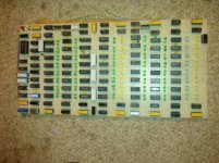
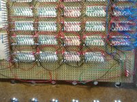
Here is a picture of the basic scheme of my Power Wiring..
So the basic rule is -- Caps are tied together horizontally with a wire and power or ground pins of the IC are tied together vertically and another pair of wires ties the cap to the IC..
The Horizontal Red's are done, now for the Horizontal black wires..
The Horizontal black wires are done, but there was only three rows of each color to do.. Where as there are mostly eight rows of the vertical rows to do in each color.. Except for the few that were done for the sake of pictures..
So, next is the Vertical rows to do in the Red.. The Red Vertical rows are done, The Black Vertical Rows are next, tomorrow..

004.jpg

THANK YOU Marty
 
Last edited:
"DDS, Thank You, for saying that This project is getting interesting..
Right now while I am in the thick of Power Wiring, Interesting is not the Word I would use.."

--

I've heard there's a traditional Chinese curse that goes: "May you live in interesting times!"

Another "interesting" favorite:

"Please, Spock, don't say its fascinating!"

"No, Doctor, but it is interesting."

I've got a ton of other stuff to do, including a bunch of computers to fix, but somehow I keep circling back to the LD12 documents. Maybe it's closer to fascinating than interesting. ;-)
 
Hi All;

DDS, "" I keep circling back to the LD12 documents. Maybe it's closer to fascinating than interesting. ""
That may be closer to the truth, than You may think..
I think this is the longest that I've been working on one project, and keep on coming back to it..
I do get diverted some, I want to make this work, and know how it (a computer) works at the Hardware level.. This is my second attempt..
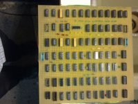
The first one was a TTL Cpu, that spanned about four Large Boards, and plenty of cables connecting everything together.. It worked, but not very well, I think there was too many un-reliable connections.. Every Register had a set of Led's next to it to show its contents..

001.jpg 002.jpg 003.jpg

004.jpg

There was another picture, but either it won't load, or it is a bad picture..

THANK YOU Marty
 
Last edited:
Hi All;

This is not Dec related, but, I thought it would help me on my PDP issues, both 8 and 11..
Here is a link for one of my diversions, I have been watching this video for the last few weeks..
And this morning I finally got it completely working, it helps me Understand about the workings of the stack..
And by getting it working myself, I have a better understanding, than I would by just watching the Video..
His Language is on the Course side, but I like His presentation.. Enjoy !!

https://www.youtube.com/watch?v=OjaAToVkoTw

THANK YOU Marty
 
I fixed a few of my 'goofs' in my LOGISIM schematic and have now got it running the MAINDEC-8i D01B diagnostic without errors (on the first attempt even).

I am calling it a day whilst the going is good!

Tomorrow I will try D02B which I am sure will identify a few problems.

I did have a look at 'fixing' the silly flip-flop clear with this daft SN74L00 device. It would definitely not run within LOGISIM. The clock edge and the flip-flop clear occurred at (effectively) the same 'time' within the LOGISIM simulation - so nothing actually happened (i.e. no register load occurred). I added another SN7474 package and a 7404 inverter gate to create a CLOCK_L signal that was guaranteed to be half a clock pulse delayed from CLOCK_H. This seems to work very successfully in LOGISIM - and I suspect to should work admirably in real life. The slight drawback is that the main clock has to be twice as fast as the PDP-8 system clock (the first 7474 F/F acts as a divide by 2). I think you should also be able to get rid of the SN74L00 as well.

Dave
 
Hi All;

Dave, Thanks for getting it running..

Remember, that the clock is anything I want it to be, as it's a 555 followed by an 74H00 and then some 7404's tied in Parallel, for Driving capability.. The clock L signal is one Gate behind or one gate ahead of the Clock H signal.. I can't remember which..
I had intentionally set the set of resistors for a very low clock rate and , the high and low of the clock signal were of the same duration.. Which also, may have been some of my problem..
I can check with a scope and see what my Frequency is and I can change the Duration times of the high against the low portion of the clock signal..

THANK YOU Marty
 
The fact that CLOCK_L is 'one gate delayed' just means that it is 'bodged' rather than 'designed'...

I have just sent you and DDS my latest LOGISIM which runs MAINDEC-8i_D01B and almost runs D02B. It 'jams' because it is waiting for the TTY interface (that I have not implemented so far yet).

Something 'strange' happened to my e-mail account - so if you don't get the e-mail please let me know and I will resend it. The e-mail contains my complete LOGISIM design and the libraries I use plus a DEC diagnostic that you can play with if you can get LOGISIM to run...

If you look in the upper left-hand corner of PDP8-LD12-PDP.png you will see my clock logic which guarantees (!) a delay between CLOCK_H and CLOCK_L (i.e. designed not bodged - maybe!).

Enjoy,

Dave
 
A quick question Marty - where do you get your large lumps of prototyping board from? I can't find these for love nor money.

Dave
 
Hi All;

Dave, Thank You for the work and effort..
"" where do you get your large lumps of prototyping board from? ""
I have two or three around here that I keep on reusing.. I originally got there from my local Electronics store.. But, I haven't seen them in awhile.. So, maybe they are no longer made in this size.. They are 8.5 inches by 17 inches perforated board with 1/10th inch holes..
I will look in a minute and see whether I got what You sent or not.. I have them..
I have about 7 more vertical rows to wire for ground, and then I can do a smoke test and see if I can fry my Power Supply or my Board..

THANK YOU Marty
 
Last edited:
Hi All;

Dave, Thank You for the work and effort..
"" where do you get your large lumps of prototyping board from? ""
I have two or three around here that I keep on reusing.. I originally got there from my local Electronics store.. But, I haven't seen them in awhile.. So, maybe they are no longer made in this size.. They are 8.5 inches by 17 inches perforated board with 1/10th inch holes..
I will look in a minute and see whether I got what You sent or not.. I have them..
I have about 7 more vertical rows to wire for ground, and then I can do a smoke test and see if I can fry my Power Supply or my Board..

THANK YOU Marty

Maybe this one?

http://www.digikey.com/product-detail/en/169P84WE/V1011-ND/38869
 
Hi All;

DDS, Thank You for finding this, Yes, This is the one..
On another note, I got the power and Ground wired, and Nothing fried..
Now to start wiring row B..

THANK YOU Marty
 
Hi All;

What do I use to view the Schematic from Dave's Logisim file ??
I think that when I try to view it, it uses something from Microsoft that shows the schematic, and I can view the center of the schematic, but that gets smaller and smaller as I increase the magnification.. And I can't move to where I want to look with side bars..

THANK YOU Marty

There's a lot of blank space there. You have to click on the screen and drag the little hand icon in the direction you want to slide the "virtual paper". And a lot of it you have to do blind because the screen will be blank.
 
Hi All;

Thank You, DDS for Your reply..
I'LL try it again..

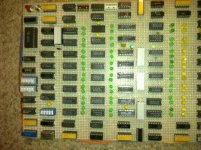
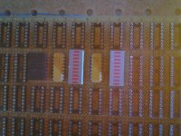
Here is a picture of some more LED's that I am adding, they are not needed, but are for Debugging..
They are left to right CP0-CP7, A0-A9 and F0-F10, I know there is an A10, but I don't think it is used, and F0-F10 are eleven places..

001.jpg

I have CP0-CP7 working on its display.. At first I had only CP0-CP3 working, but I found that I had a short, a wire not completely wrapped on it's pin.. I have also added another LED for F10, below the right R-pack..

THANK YOU Marty
 
Last edited:
The fact that CLOCK_L is 'one gate delayed' just means that it is 'bodged' rather than 'designed'...

I have just sent you and DDS my latest LOGISIM which runs MAINDEC-8i_D01B and almost runs D02B. It 'jams' because it is waiting for the TTY interface (that I have not implemented so far yet).

Something 'strange' happened to my e-mail account - so if you don't get the e-mail please let me know and I will resend it. The e-mail contains my complete LOGISIM design and the libraries I use plus a DEC diagnostic that you can play with if you can get LOGISIM to run...

If you look in the upper left-hand corner of PDP8-LD12-PDP.png you will see my clock logic which guarantees (!) a delay between CLOCK_H and CLOCK_L (i.e. designed not bodged - maybe!).

Enjoy,

Dave

One possibility would be to dummy in something that responds just enough to make the DEC diagnostic happy. Then do the full TTY interface at a later time.

Also, if you look at the lab manual on figure LD7 on the bottom of the page you'll find the author's CLOCK BOOST schematic. It's only partially labeled but there's enough there to guess a few things. Notice on the right of the page, after the signal gets branched out to become "Clock lo" and "Clock hi" the Clock lo path has two effective gate delays while the Clock hi has only one. This would guarantee that a pulse on Clock lo would be one gate propagation delay time behind Clock hi. The amount of delay in nanoseconds would vary by chip type, not by clock frequency. I have no idea at this point whether the author's design needs the skew or whether he was just trying to save a few gates. But note that he does a similar thing when generating CPnh from CPn on figure LD9. When I see two signals that are labeled as if they are the Boolean inverse of each other I tend to assume they are symmetrical. This design has a few quirks that I would have avoided. The material is confusing enough without adding stuff like that. Were I in his class I would have been unhappy having spent good tuition money to be there.
 
Hi All;

DDS, If I remember correctly,, "" I have no idea at this point whether the author's design needs the skew "" I read that if there is a problem with skew, that a different part could be put in.. Also, remember that in His design, the the Gates for Clock.Lo had two parallel gates for Loading.. And the Clock.Hi had four parallel gates to accommodate all of the Loads that it needed to drive..
I have on my design, put the clock on the same Ic.. And I did the same type of thing on the Cpn's, I used two IC's just for the CPn's, so that I could put in anything I wanted, whether plain 7400 or LS, S, F.. And it would affect only those signals..

THANK YOU Marty
Yeah he has both lines running through parallel inverters to be able to drive more than the normal number of gates downstream. The Clock lo goes through two while the Clock hi goes through four. The skew comes from the extra nand gate that Clock lo goes through before it gets to the two parallel inverters.
 
Hi All;

DDS, Thank You for the information..
"" The skew comes from the extra nand gate that Clock lo goes through before it gets to the two parallel inverters. ""
I have an 74S00 there at present, But, I can change it to an 74AS00, an S is 3-4 nanoseconds, and an AS is about 2.5..
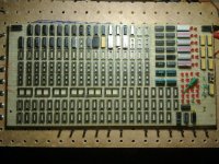
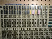
Anyway, here are some pictures, on my progress, Today, I was gone most of the Day, so I made very little progress..
LD-8 is mostly wired and some of LD-9 as well..

002.jpg 003.jpg


THANK YOU Marty
 
Hi All;

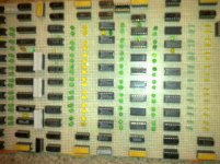
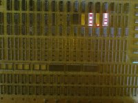
Here is another picture, I have wired up the An, and the Fn, driver wise, and so all of the correct Led's are lit..
The one's that are not lit, are not connected, and are not used, so there is no use wiring them up at all..

002.jpg

THANK YOU Marty
 
Back
Top