• Please review our updated Terms and Rules here

VT180 repair. Clues please.

acollins22

Experienced Member
Joined
Mar 12, 2007
Messages
257
Location
Leicester, UK
Hello Folks,

I am trying to repair my VT180 for this year's Retrochallenge.

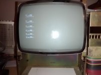
So far I have proved the voltages to the boards are OK. I am trying to get the VT100 side working first and then the VT18x board and so I have just got the VT100 part on its own (connected to the monitor). I get a poorly synced display of garbage multiple times down the screen.

I have removed the extended graphics card so that I can get to the processor and I have also removed the comms board that links the VT100 to the 18x. This hasen't made any difference.

The CPU seems to be running, there is activity on the bus. However, I don't see much change on the data bus. It could be stuck in a loop waiting for the keyboard but I don't seem to see any activity on D4-7 (IIRC, not near it at time of writing!)

Please could someone give me some clues as to what to looks for on these? I have a 'scope and soldering kit and I'm not afraid to go in!


Thanks very much.

Andy.
 
What kind of instruments do you have to analyze the problem? I would attach a logic analyzer to the address bus to see what addresses it accesses. It sounds strange that D4-D7 is not changing. Is this on the processor itself? Are you using an oscilloscope to measure the data bus?

If there is a problem with the PROM contents you can end up in all sorts of problems I guess. I think that the VT100 ROMs are dumped somewhere. It could be useful to compare the contents of the ROMs so that there is not bit-rot that is causing your problem.

I will soon be looking into one of my VT100 so we'll see what kind of problems that I get when dealing with it.
 
Bit rot! do you run into this often? Wonder if I should be making copies of some of my ROMs around here? Don’t think I have yet come across a bad ROM but maybe I am a lucky guy? Have all he tools in an archaic ProLog 980 ROM reader and writer and a sack full of 2716 and 27128 chips.
 
For some odd reason, the VT100 character generator rom is failure prone. We have seen it here on the forums a few times. Here is the mod to replace the chargen rom in the field with an EPROM: http://www.vintage-computer.com/vcforum/album.php?albumid=58&attachmentid=4647 of course you have to program the eprom, but that is trivial.

Andy, please get the VT100 technical manual and the print set off of bitsavers.

There could be two problems. The poor sync could be on the analog video board, while the rest is on the VT100 board.

If you have a baseband NTSC monitor, drive it from the BNC output on the back of the main board. If it synchs well, then the analog video board that drives the CRT will need investigating.

The VT180 always has the AVO option. For the screen garbage problem, it is worth trying to remove the AVO to see if the problem goes away or changes. I have seen a bad attribute ram on the AVO.

Please take a photo of the screen of garbage and post it here. I have repaired most video terminals from VT52 through VT278. It may take us a little while since I have a day job, but we can get that Robin working again. This was what it took to fix my Robin: http://www.vintage-computer.com/vcforum/album.php?albumid=56&attachmentid=2421 .

Lou
 
Last edited:
Hello everyone and thank you for your replies.

I only have a 'scope at the moment and the bus activity was monitored on the pins of the 8080.

Andy, please get the VT100 technical manual and the print set off of bitsavers.

Yes, I have the technical manual but I don't know what you mean by the "print set". Please explain.

If you have a baseband NTSC monitor, drive it from the BNC output on the back of the main board. If it synchs well, then the analog video board that drives the CRT will need investigating.

Sadly, no NTSC. I'm not too worried about the video side of things at the moment. I think the garbage is the bigger problem.

I have removed the AVO board but there was no change.


This was what it took to fix my Robin:
That photo gave me great confidence as I had decided to take the board from the frame as I thought that the cable and backplane were straight through and passive. Thanks for confirming that!

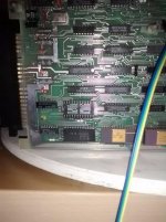
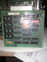
Here are a few photos of where I am...

160106-IMG_20160106_194705.jpg160106-IMG_20160106_194732.jpg160106-IMG_20160106_194827.jpg


Thanks,

Andy.
 
Andy,

By print set, I mean the schematics. Here is the link: http://www.mirrorservice.org/sites/...minal/vt100/MP00633_VT100_Schematic_Feb82.pdf .

Yes, sadly no NTSC on your side of the pond. A multi-standard TV might be a good addition to your toolkit at some point.

So when I look at the "garbage" I think of two things. First, the top row of garbage is large and bold, and the row below it is small. This reminds me of the "setup screen" that shows "SET-UP" in big letters, with smaller text below it. So you must tell me more. 1. does this same screen come up every time you flip the mains switch? 2. do you have the keyboard plugged in? 3. How does the screen change when you first power up the machine and then press the setup key? 4. If you connect a loopback plug (pins 2 and 3 tied together) and you start typing on the keyboard, can you see more or different garbage appear?

The repeated pattern is also interesting. Are we seeing multiple frames on the screen at the same time, or is this one frame with the "garbage" pattern repeated. So, crank up the brightness until we can see the raster and the garbage. If this is one frame, then the distortion is easily fixed with adjustments on the analog video board. Start reading the technical manual sections on the analog video board. If you fiddle with the pots, keep track of where they were when you start, and put them back.

Lou
 
Hello Lou,

Thanks as ever for your suggestions.

In answer to your questions..

  1. does this same screen come up every time you flip the mains switch?

    Yes. It's the same each time.

  2. do you have the keyboard plugged in?

    I didn't when I took those photos but I have plugged it in tonight and the results are the same. Also, All of the keyboard lights come on. When I started a few days ago, I remember that it beeped and only a few of the lights came on. Something changed but I'm not sure what yet.

  3. How does the screen change when you first power up the machine and then press the setup key?

    There is no change.

  4. If you connect a loopback plug (pins 2 and 3 tied together) and you start typing on the keyboard, can you see more or different garbage appear?

    Again, no change.

Those tests were carried out with both the AVO and small comms board removed.

I now have the schematics. So I'll be looking through them :)


Cheers,

Andy.
 
Hi Lou,

Ok, it now sounds as if the 8080 controlled portion is not passing its power on self tests. Do all of the keyboard lights come on and stay on after you power up?

Yes. All of the lights on the keyboard come on and stay on.

On a side note I have borrowed an 18 channel USB logic analyser over the weekend so hopefully I can use that, with your guidance, to shed more light on the problem.

First try shows all bits on the data bus are being used. Somehow I got mistaken using the 'scope.

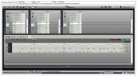
I have attached three screen shots taken of the logic analyser screens. I have 18 channels and so I have the data bus, the lower 8 bits of the address bus and the synch pin. All signals are from clips on the 8080.

I have the triggers set to stabel high on sync (start of new instruction) and 0 on the address bus. I put the analyser to wait for trigger and turned on the VT180.
The three shots are from the same run and I've just stepped through the time a little to show what happens at start up.

vt180-digiview-1.jpgvt180-digiview-2.jpgvt180-digiview-3.jpg


Cheers,

Andy.
 
Last edited:
I quickly checked this bin-file towards what I see in your analyzer trace. The first few bytes seems to be the same, i.e f3 31 4e 20. This corresponds to a di and a ld sp,0x204e instruction. But then at address 4 there is a c3 in the dump while I understand that in your VT100 it access a c7. I am not sure if this because your firmware is different from the dump or something else. c3 is jump instruction while c7 is a rst 0 instruction, but I am not exactly a 8080 guru...

Anyway there are some interesting things written on this page: http://vt100romhax.tumblr.com/.
 
According to this page there appear to be two different variants of the lowest ROM. One is 23-031E2 and one is 23-061E2. The dump I referenced previously seems to be the 23-061E2 variant. You might check what kind of ROM you have. The ROMs I had were also 23-061E2.
 
I have now started working with the VT100. I hope you don't mind if I hi-jack your thread a little bit.

Anyway, the PSU looked fine on the bench with a variac and bench supply (for the 12V startup voltage). It delivered the 5V and regulated well. So I put everything together and hit the power button. The keyboard blinked and there was a beep. A good sign. After quite a while there were a very dim display. The keyboard was sort of not working well but it was due to bad contact in the connector. Some Deoxit seems to have solved this. Then the SETUP key didn't respond every time. But I think I need to dismantle the keyboard and check the switches.

But after a while there were coming this burnt smell. So I switched of and investigated. It was the same resistor in the PSU that had became slightly hot when bench testing that now were even hotter. It's the R27, a 1kohm 13 W resistor. In the schematics it says 500 ohm, but mine is 13 kOhm and it looks like it is not replaced but the original. Maybe some kind of revision change. At least the +5V looked fine when the Vt100 was running. Measured 4.99V at one 74LS00 chip.

Does anyone know if this usually gets hot? It was so many years ago that I switched on a VT100 so I don't remember the normal "smell" from them any longer. Or is this in fact a sign of imminent failure of the PSU?
 
With the power supply running measure the voltage across the resistor. Measure the resistance with power off (assuming you can without desoldering one end to remove any parallel resistance in cicruit). Then compute the power the resistor is dissipating using Ohm's law P=V^2/R. It should be less than 13W be a good margin. If not, that is why the resistor is getting too hot, and either the voltage across it / current thru it are too high for the current resistance value.

Don
 
The problem is that this resistor is part of the snubber network on the primary side. The currents and voltages are not DC or sinusoidal AC, but pulsed DC. I think that there will be a current peak whenever the the switching transistor turn off. But getting a good reading of the voltage using my multimeter is hardly possible. A scope could be used, but I think a lot of the energy is in the short spike which could be hard to catch. I have a current probe which is probably the best tool in this case.

VlInF90.png


One question that I have is why they changed the value of this resistor. What is the value of R27 in other VT100 PSUs? 500 ohm as in the schematics or 1000 ohm as in mine.

What is the situation with those of you that have a running VT100. Does this the R27 resistor get hot?
 
Your comments are correct; I was under the assumption that the resistor was in a low voltage circuit with a low frequency application where a DC analysis is realistic. Not so it would appear in this case. You would need a scope with a high voltage probe capability (that is a 600V diode and 1600V capacitor in the same circuit) so it could have very high voltage, very short duration, pulses across it. Much harder to measure the power in that case.

Don
 
What kind of problem in the circuit above would cause R27 to dissipate so much energy? Could there be a problem with D27? But normally what is interesting with these diodes are that the trr is short so that they do not conduct in reverse for such a long time. And if they do they usually break.

The circuit is not that complex and I cannot figure out a component that would cause excessive power dissipation in R27. Film capacitors seldom break so it is unlikely a problem with C19. T3 is probably either working or not. Then there is the network of diodes on the base. Could any of those cause this?

If I are to measure on R27 I probably clip on my P6042 current probe. It should be very useful here. But then do all the math to get a accurate power reading is not that easy.
 
No, C19 is not shorted and D27 has a measured Vf of 0.451V.

Can C19 be marginally bad somehow? It a Sprague 0.0033 uF 1600 VDC capacitor.
 
Back
Top