• Please review our updated Terms and Rules here

Project to create an ATX 80286 mainboard based on the IBM 5170

A small status update for those following this project:

I have completed the mainboard PCB layout. Currently I am doing the whole "start to end" verification of the prototype schematics including the CPLD logic. After that is done I will create the RAM PCB layout and order the PCBs.

I am also ordering some CPLDs and the Atmel USB JTAG programmer as discussed earlier in this thread. I ordered it previously but it failed to deliver because of DHL messing up the delivery, so now I am going to order again this time from Mouser. I also bought some CPLDs and 16Mhz 286 CPUs from a Chinese Ebay seller and I will find some more sockets and stuff from Ebay. I will at least have some genuine CPLDs from Mouser and I will see if those from the Chinese seller are okay too, I saw that other buyers verified them to be fine.
 

Attachments

  • 286 AT PC ATX mainboard Rev 1.png
    286 AT PC ATX mainboard Rev 1.png
    219 KB · Views: 23
  • 286 AT Project PCB Layout print.pdf
    699.7 KB · Views: 4
Can I just say this is a very cool project, all the best with it - your other 8088 boards look fantastic, as someone who made a 8088 computer (XTjr based on the Xi8088) much more professional than my jobbie!

Im also looking into using Atmel ATF15xx CPLDs for one of my other projects, and as I'm a massive cheapskate, I've seen that you can use the very cheap FTDI FT232H boards to program them using OpenOCD and a tool to convert he JED to SVF, as described here on by hoglet on the Stardot forums:


Might be good as a backup should the next Programmers delivery go astray... I'm not sure how much the programmer is, but Vendor cables can often be pricey.

Anyway, sorry if this has been covered in this thread already and I missed it...
 
Hi mogwaay,

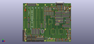
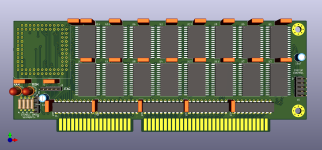
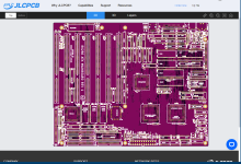
It's really great to hear from you here! I am always glad to talk with someone who has the same deeper interest in these historical vintage computers, which is also my reason for being here. Sharing ideas and inspiring eachother is what it's all about for me. I appreciate the compliments, thanks for that. I always feel I can do it even better in my designs because I will be paying the factory for making the boards, I always try to get the best result out of this service so it's hard to stop reworking the layout but I must force myself. My time should be limited because at the same time I want two things to happen, to have a result which feels right and I also need to drive this project to an actual result. For the mainboard I did get to the point where I am happy with the result. I am doing a lot of design verification work at the moment, trying to make as sure as possible before hand that the project has the best chance to function correctly, it is a very complex project.

I think I found your project at GitHub, it looks really interesting and I can see what your vision has been to create a kind of "home computer" style with only the things it needs and it looks like you did a nice job to realize it! I do love the idea and I also have some plans to revisit certain computers in a different form. I still want to do a "pizza box" format computer design and I plan to redesign the Amstrad PPC640D to replace the whole PCB inside mine with a single one. I am not sure if I will be using their chipsets on the new PCBs, or to possibly replace these with something else.

Next to the projects you have seen so far, I am also working occasionally on another 8088/V20 design with my daughter based on the 5150, specifically because it supports tape I/O which I want to play around with. In fact, looking back I am thinking I could have done this in the first place with my XT originally. At the time I was not sure about the differences of design between the 5150 and 5160 because I had not worked with the XT and PC schematics as much yet, so at the time I chose the 5160 because it was newer and could be possibly better. As I now have much more insight into the PC and XT logic, I could just as well have chosen the 5150 as a basis for the project. Fundamentally only the interrupt controller is wired and programmed differently in the 5150, and the IO space in the X-bus is more limited which can be changed of course. Maybe I will make a layout with footprints for both methods of programming and connecting the 8259 in case I need that later.
With a few small tweaks I believe it doesn't pose any compromises to go with the 5150 circuits in certain areas, while gaining the added advantage of the tape capability preserved. I want to experiment a lot with tape I/O in DOS as well. Like creating a file from a tape, or creating a tape from a file directly in DOS. Also I want to do advanced tape I/O monitoring by sound and LED indicators just to enjoy that retro experience of using a tape more. I have seen a Chinese ebay seller who is offering a lot of traditional analog tape circuit ICs, maybe new old stock, which may even make it possible to do some custom work on a tape drive, though I am not an analog expert, but I can get more experience and study existing tape drives of course. This project of a 5150 based mainboard is in the making and I will publish it later. It will also feature a RTC and some other enhancements. I bought a IBM 5150 "tank" case and power supply shell which I will design the PCBs for, just for a retro look and feel, and I will also do a redesign and create a 6845 based video card to be able to connect this setup with a CRT. More about this project later when it's done. That mainboard will also be ATX powered using a good ATX power supply transplanted into the original IBM PC power supply housing. At the same time this mainboard will be very integrated and feature "only" 5 expansion slots to match the 5150 case which is of course more than enough especially on an integrated mainboard.

Thanks for your suggestions about the alternative programmer and software method, that is really helpful info and I was not aware of this. I will look into it later as a possible alternative. If I can cut some costs in a good way, I am also in favor of that. This project has already cost me a lot, especially loss of sleep working at night on the project so many times. ;) I will probably order the programmer that you mentioned as well now that I know this alternative exists. The one at Mouser is expensive, you are right, it lists as 93,59 euro in the Mouser shopping cart so it will cost me. Right now I just don't want to risk anything which could end up delaying the project unnecessarily for any reason. When I have a safe and good method to get the CPLDs working already, I can also do more testing later to compare if other methods also work just as well as the official one. I will share my CPLD experiences here and I will also read and research the thread from your link later, I will keep this in mind so thanks for that mogwaay!
 
I just ordered only the Atmel USB programmer from Mouser, I decided not to order any CPLDs from them because the faster ATF1508 they were selling was a 3.3V only type(ATF1508ASV), and the 5V type they did have in stock was a slower ATF1508ASL 25ns part. The price for the programmer was even a little higher at checkout because of added VAT costs.

So I will be trying the CPLDs from the Chinese ebay seller which support 5V and are 10ns speed rating.
The type indication is: ATF1508AS-10JU84.
So this type supports operating at 5V directly and is more ideal for this application.
I expect anyway that the Chinese sellers will offer the ICs for a longer time period than Mouser and similar sellers.
Of course when buying from those it's a bit of a gamble but it can be a good indication to check the reviews of other buyers from the particular seller to have a better chance of success.

Mouser lists the correct datasheets with each product in their system, where there are very subtle differences found in the descriptions.

Also the number of erase operations on this ATF1508AS are much higher because it is a "EE", Electrically Erasable, type of chip technology.
This features a number of erase and program cycles of around 10000 compared to around 100 for a "E2" erasable type of chip technology, possibly listed as "JC84" or "JI84" at the end of the type indications.
Of course this is also sufficient for this mainboard anyway since after the prototype is verified there are not so many erase operations expected to be necessary anyway.

Since I have not tested the prototype I want to test first with the faster rating ICs so I can have the best chance to possibly clock the CPU at a higher speed when the prototype is fully working.
Later if I have the chance I may possibly do more testing with slower types of CPLDs to see if they can be suitable for a standard operation for example at 8Mhz, comperable to the 5170.

So this is an important aspect to keep note of to carefully check the type indication to make sure it's a suitable CPLD chip.

Of course, to redesign the PCB layout for using some different form of CPLD or other programmable logic, in case that becomes an issue, is relatively a little more easy to do than an entire redesign of the whole PCB because it only requires to change the PCB layout in a smaller section of the mainboard. Traces coming in and out of that area are mostly running to the CPLDs.

If I need to change chip technology for any reason I will probably switch to an even lower voltage CPLD type and feature it on a plug in PCB using level shifters. Or even possibly use some kind of readily assembled adapter board for an FPGA solution. In that case I will use a single chip with a larger pin count instead of the two PLCC types, which are still the preference for now because at least they can be plugged into through-hole sockets which is much more convenient to handle.

So I will post my experiences here in case anyone is interested to also build this mainboard so you can know what type of CPLD will be needed.
Chip availability is indeed an issue and consideration with CPLDs so I will update my findings in this regard in more detail later.
 
Hi Sir_Fartalot,

Thanks a lot for your message and encouragement, I appreciate that you're interested in my project!

Kind regards,

Rodney
 
Today I received the Atmel/Microchip original USB JTAG programmer from Mouser.
So this is great to get one after the last mishap with DHL.

I can say one thing in favor of the added costs, the original programmer comes in a strong plastic housing which makes it easier to handle.
It is not a justification to pay a lot more as I have, but since I already paid for it, it is an advantage worth mentioning.

At the moment I am working on all the design verifications.
I also rewrote the U87 logic equations with corrections which observe the correct polarity of signals. This since I am not using a PAL, instead U87 is a part of the System controller CPLD.
After I double checked everything in several ways, I will get to work on the RAM card design.
Then next it will be time to order the prototype PCBs for the mainboard and RAM card from JLCPCB.
 
For everyone who is interested in my project and those who helped me in this thread a small progress update.
I am working hard on the project, I have verified all the schematics and double checked all my work. Everything looks in order, I could not find any issues.
Basically I followed the entire development from start to end another time and cross checked against the 5170 schematics on paper.

I finished the memory card design and I am almost done with the PCB layout. I condensed the layout and I will be using 4 layers for the memory card as well.

So this card contains 30 SRAM chips of 512KB each, so maximum of 15 MB which is the memory layout specification for the 286 AT. The gap at 15-16MB is reserved and intended for example for VGA cards which can map their memory into that space if it is designed that way and other memory mapped cards if needed if those operate in this reserved space.

I will finish the memory card design as soon as possible and then do a short verification before ordering the boards from JLCPCB.
In the attachments a few screenshots of the memory card to get an idea of the design what it looks like.

I know some people may not like to solder smd stuff however this design is made for extra easy soldering of the smd ICs, the pads are extra long to accommodate all variations of width and can absorb a lot of solder. Using a thin soldering tip and thin leaded soldering wire to carefully dose the amounts of solder to each pin, it is quite doable even if you never did that before. I can really recommend to try this first before resorting to DIP SRAM which is much less ideal.

For those who really don't want to solder any smd parts I may design another card later for using normal SRAM, though those are really much larger in size and hard to get original parts which are not fake. So we can discuss here later about this, I will try to accommodate those who want to use normal ICs if necessary so if you really want to build this project with DIP SRAMs we can discuss here later about this how we will do it, however it will take some development time to design a possible PCB if necessary.

First thing is to build the project soon and verify everything for proper operation. I will need some time after it is operational to test out different software and adapter cards and scope out the ISA slots to see if anything needs further cleaning up because of crosstalk and reflections in the lines. I already provided capacitor footprints to clean up the typical lines which I found before on the XT to be noisy and sensitive, especially positive polarity input signals of the system. I expect this system to be much less noisy thanks to the improved ground planes because of using a 4 layer design. I will opt for the normal thickness of copper on the inner layers just to get a really solid and strong PCB of decent quality.

Kind regards,

Rodney
 

Attachments

  • ISA Memory subsystem Rev 1 bottom view.png
    ISA Memory subsystem Rev 1 bottom view.png
    88.8 KB · Views: 14
  • ISA Memory subsystem Rev 1 top view.png
    ISA Memory subsystem Rev 1 top view.png
    125.3 KB · Views: 14
Last edited:
Rodney, many thanks for explaining all the ISA bus details - quite a while until I found enough time to thoroughly read through it.

I was really concerned that this RAM connection choice reduces RAM performance, but it really doesn‘t seem warranted.

Is SAx/SDx then directly connected to Ax/Dx, so no delay is introduced?

Watching a lot of retro stuff on youtube, I wonder why most memory expansion cards shown there have a proprietary connector? I also remember one video saying “do not use a ISA-only memory expansion card on anything later than a 6/8 MHz AT, or memory access will be slow“ - this is plain wrong then, right?!

Cheers,
Johann
 
Hi Johann,

It's great to see your message. You are quite welcome.

Yes, the SAx/SDx bus is directly connected and following the Ax/Dx bus while the CPU is active. During different bus modes there is always a direct control of all the buses involved in the AT system. One bus controls the other always in a direct fashion, simply put.

During CPU control the lower SAx lines then go to the RAM chips through transceiver buffering, the highest Ax lines only go directly to the memory decoding logic for selecting the proper RAM chips for each memory region.

During DMA by the two 8237s it's a little more involved, amongst other mechanisms, the XAx/XDx bus is used to control the SAx/SDx bus by reversing the transceivers and the memory mapper is programmed to control the highest Ax lines to access memory through the memory decoders via DMA paging method. Various control lines of the system are also reversed with their "X" versions. So the DMA method has some mechanism using programming and paging which is less direct than the CPU, but more suited to transfer blocks of memory more quickly and more simply because it needs less cycles.

As I mentioned, the SAx/SDx bus is not a "ISA bus" persé, but better to be called a "system bus" which I believe is the purpose for the "S" naming convention of the signals.

In the AT PC it's the intention of the design that all memory be controlled on the "S" bus. On the 5170 the onboard DRAM also is connected to the SAx/SDx bus and then multiplexes to the DRAM lines with MAx names. I am doing the same thing on the memory card except for multiplexing is not needed, the SAx/SDx bus is connected to a MAx/MDx bus on the card. The highest CPU lines are used directly for decoding and selecting the correct RAM chips for each memory area. This is replaced by the 74LS612 memory mapper chip during DMA, and reversed to a bus master DMA controller in an ISA slot if needed. So we use these LAx lines to control the memory decoding. The LAx bus follows the Ax bus directly during CPU and onboard DMA page register access. If there is a bus master ISA card, it can control the memory decoder CPLD through the LAx lines as well to access all the RAM on the card.

So whether we connect the RAM on the mainboard itself or on a slot connector doesn't make any difference connection-wise. I don't mind repeating this point just to make it more clear. The ISA slot connector exposes a number of the AT system signals which is designed to be sufficient to cover all possible types of conventional expansion cards.

If a more tightly involved connection with the system is needed, a few more signals can be connected from the AT system as a supplement to the ISA slot connections.
Which is what I did in my design as well with the memory card.
Some signals I used directly in my 10 pin custom connector to the mainboard are not really needed because the ISA slot has functional equivalents, but I did it anyway because it allows for a faster and more direct response of the memory card which may help to raise the maximum possible clock speed by setting up the SRAMS more fast. The 10 pin connector contains a few other necessary signals which are needed in my chosen configuration of the system. Some design choices I made were related to the number of usable pins in the 84 pin PLCC CPLD package. Which resulted in the design as it is now.

There is always a propagation delay for any computer system, this is unavoidable and not a problem because any computer system deals with this principle.
Bus transceivers usually have a very short and fast propagation delay compared to other TTL logic chips so connections are fairly direct and instantaneous.
If we want faster transceivers it could possibly be advantageous to use CPLDs for the transceiver functions as well.

When I started this project of this thread quite a while ago I had a certain vision for the design.
What I wanted was to recreate the IBM 5170 16 bit design for several purposes:
- historical preservation and documentation of the technology
Recreating the system in a fully documented manor is another method to accurately record the entire technology principle. And if it functions properly, this is also serving as the proof of concept to be accurate.

It's essential to discern here between recreating a system using chipset logic of which the contents is only known to insiders or a manufacturer, or recreating a system where all the logic is fully documented and openly available for study by anyone who wishes to do so. Which is what I am attempting to do. Definitely this could be valuable for academic purposes as well.

- learning about how IBM implemented the perfect 8 bit compatibility in their 5170 system
We cooperated to define the PAL logic in U87 which is an essential part of this mechanism. By cracking open the last puzzle piece of the PAL logic we succeeded to openly document the entire IBM AT system for the first time as far as I am aware of. After doing extensive research I was not able to find the entire AT design anywhere. I mean, there is still some design aspect contained in the PROMs but this is really minimal and I already replaced these PROMs in the CPLD designs. The PROMs can be read out so it's nothing hidden or illusive there. Understanding the whole system how it operates is now possible because we have a fully complete schematic. Besides studying all the logic, one would also need to study the Intel documentation of the CPU and support ICs. Then you can get a functional complete and comprehensive picture of the system.

IBM really did an exceptional job to create a full system more or less according to how Intel had envisioned the usage of their 286 CPU. I mean, it's not a multibus system as Intel describes but except this aspect, IBM surely succeeded in getting the full range of use of the CPU as designed by Intel. I think IBM was absolutely the best manufacturer in those years capable of creating such a system and standard. I noticed a few details recently in the CPU control support logic which made me realize that IBM was closely observing the Intel CPU documentation in their design.

- getting more hands on experience and insight into the AT PC
When looking at the AT PC now, it is much more familiar to me and more deeply understood by having more comprehensive practical insight. That is what I wanted. To be able to look at the system and know it deeply, similar to what I did with the XT, though the AT involved much more complexity. The better I get familiar with the AT system, this can also result in other methods to implement it in new resulting designs in the future.

Here we now are attempting to create an AT system which is at least capable of relatively offering a reasonably large amount of RAM memory if so desired. Basically when you build this system you can choose how much RAM you want to put on the card, from 1MB up to 15MB of total RAM. I yet need to find out how the BIOS responds to increases of XMS memory being present on the system. I will start with 1MB of RAM and then add more chips to see how the MR BIOS responds to the changes.

The 16 bit memory principle allows twice faster memory response times compared to the 8 bit XT because it reads two 8 bit bytes at a time during each CPU cycle.
So this speeds up programs running in the 16 bit memory.

Next we have the CPU speeds themselves. I predict there should come a limit of around 12-16Mhz for the CPU speeds using the SRAM chips I have here.
Maybe higher since I think SRAM is better than DRAM in principle because it's more directly controlled with simpler access timing and less impedance difficulties.

When CPU speeds are raised, there will come a point where the SRAM is not accurately providing the data anymore due to insufficient setup periods for the data bus to stabilize for reading by the CPU which will crash the system.

We can test this speed threshold of the SRAMs to find out where it lies.
Faster speed is also known to produce more heat in RAM chips, so this may or may not also be an issue to keep in mind.

When I build the prototype I will have a look at my SRAM ICs and choose the fastest ICs I can find here with the fastest access times.

It's really essential now to first get a functional system up and running.
This can hopefully validate the design which is another very important milestone in the project which I hope we can achieve.

So I will start at the original 8Mhz internal CPU clock speed in order to validate the design.
After this is done we can explore further what is possible.
If we want a faster system it would probably be better to choose a faster type of CPU technology.
For example 32 bit technology like a 486DX or similar.

Okay, I get back to work on completing the RAM card.

I already generated a set of gerber files for the mainboard so it's ready to order from the PCB house.
I will combine the mainboard and RAM card in one order so I can build up and test the system as soon as they arrive.
Hopefully by that time I will also have the required CPLD chips delivered here as well.

Kind regards,

Rodney
 
Last edited:
Rodney, thanks again for your patience. I think I slowly start to understand. :)

PS: 1:1 after 67 minutes. I predict end result 2:1 :) :)
 
Hi Johann,

I totally understand that it's difficult, so I am glad to give some hopefully useful information which could save you from needing to study schematics for many hours, which I know you don't have. ;)
And I am of course glad that you care about the project so much to have concerns about it, so I am happy to see this level of interest.

And you have helped me a lot with your very useful python programs, which saved me from needing to decode many lines of equations by hand to discover the problem with those feedbacks from OE enabled PAL functions.

I think you were hinting to some soccer matches? I must admit I totally don't follow soccer for years, especially after the Netherlands were doing so poorly in the matches, they were looking less and less like a team which was frustrating to watch at the time. :)

I must say, using those CPLDs is starting to look more and more advantageous, and I plan to do much more of this type of design in the future. Maybe I will revisit some of my previous designs to reduce the logic.

Also I am thinking about designing some legacy IBM video adapters, which also can benefit from CPLD reduction and SRAMs to design much smaller card sizes for these. I have some 6845 chips in my parts box which are doing nothing yet since I bought them years ago. I plan to find a green CRT which I currently don't have yet. I do have a CRT screen which seems to have a "green" switch on it to switch to a green-only mode which I should try out. But that design is more suited for a home computer look, not a PC. I really hope to find a IBM or similar looking cool design to match up with the IBM 5150 case design.

Kind regards,

Rodney
 
I have completed the memory card design and generated gerber files for the card PCBs.
This weekend I will order the PCBs from JLCPCB for the mainboard and memory card designs.

In the mean time I received a package from China in good order with 5 CPLDs and two 16Mhz 80286 plastic Siemens chips.
I checked the CPLDs with a multimeter and they appear to be genuine.

So now I only need to find the PLCC sockets for 84 and 68 pins and I should be able to solder and test the prototype when the boards arrive from China. Other stuff like transceivers etc I can desolder from other 286 boards.

After I have the prototype fully running, I may also look into how to modify the actual 5170 mainboard to operate with my memory card design. If this is not too difficult and involved, I may test this out. I mean, to have a 5170 with lots of SRAM is also a cool idea if the modifications would be doable.

I seem to remember there was some recompiled version of Doom which should work on a 286. Of course, it will need a lot of RAM at least to be able to even start the software.

I also want to publish all the designs on GitHub soon so everyone can see my work.

After this project is finished I will be looking into a 486 design, I am not sure if it will be 16 or 32 bit.
I need to study the Intel 486 and Vesa local bus specifications and search for chipset documentation to see if a design could be realized with CPLD or FPGA logic. If it only can be done with chipsets I don't think I would be interested in doing that.

When I look at 486 mainboards it seems like possibly the vesa local bus is tightly connected to the CPU which would make sense. Maybe in those days the chipset was mostly handling the traditional logic functions such as DMA, IRQ, decoding, byte conversion and memory interfacing etc. But of course it may be my optimistic wishful thinking.

A few screenshots of the finished Memory card design are attached to this post.

Kind regards,

Rodney
 

Attachments

  • ISA Memory subsystem Rev 1 bottom view.png
    ISA Memory subsystem Rev 1 bottom view.png
    118.4 KB · Views: 1
  • ISA Memory subsystem Rev 1 top view.png
    ISA Memory subsystem Rev 1 top view.png
    137.7 KB · Views: 1
Last edited:
I just read through the 80486 datasheet out of curiosity and if I am reading it right, and I will read it again in the future, the 486 handles data byte conversion for 8 and 16 bit reads and writes internally and generates the additional bus cycles completely by itself. Which if I am correctly interpreting the text would be a huge improvement. And of course it makes sense that such a task would be better handled internally by the CPU. This is really interesting and I can recommend reading the 486 datasheet if you are interested in the development by Intel. So there would be no external "brains" circuit required to do data byte conversions. When I look at the circuits needed for 8 to 16 bit, it would be incredibly complex to do 8 and 16 bit to 32 bit conversions externally. So the main concern for the designer is to properly interface the data bits to the correct data lines of the CPU on which the CPU expects the data bits to be connected for a particular read or write cycle in the IO or memory space. I do wonder if it would be possible to interface a 16 bit system to a 486 by keeping it forced in 16 and 8 bit modes. I think it may be possible. Not that this would be a preference, which it wouldn't normally be, but just out of curiosity if this type of system could be possible and would simplify a design just for experimentation sake.
 
I'm finishing my PAL reversing work which evolved out of this thread and would like to summarize a little...

With the help of Eudimorphodon (thanks!!) and after studying PAL and GAL datasheets, I was able to write my own simplified GAL assembler which can convert the pete.py generated equations into a flashable jed file.

What I have learned is that (unless the PAL/GAL assembler is capable of converting the equations):
- A PAL needs its output pin equations in negative polarity (i.e. "!Pin1 = Pin2 & Pin3")
- A PAL needs its output pin enable equations in positive polarity (i.e. "Pin1.oe = Pin2 & Pin3")
- A GAL has additional fuses ("XOR") which allow the output equations having positive polarity
- A GAL has additional fuses which allow to disable unused term ("product term disable fuses")
(A GAL has even more additional fuses which I will ignore here.)

I felt it would be more "retro" to NOT use the additional GAL features, so I tried to find equations which could even be directly used in a PAL. Interestingly, both U87 and U130 include some tricks which lead to the pete.py generated equations not being directly usable - see comments in the pld files:

U87:
Code:
!END_CYC = Q4
  # AIOW & !RES_0WS
  # RAS & !RES_0WS
  # FSYS_16 & Q1 & RAS
  # AIOW & Q1 & !IO_CS_16
  # Q1 & !IOR & !IO_CS_16;
END_CYC.oe = 'b'1;
!DMA_AEN = !AEN_1
  # !AEN_2;
DMA_AEN.oe = 'b'1;
!XA0 = 'b'1;
XA0.oe = !AEN_2;
!XBHE = XA0
  # !AEN_2;
/* pete.py output:
XBHE.oe = !AEN_1
  # !AEN_2;
*/
/* "fixed": */
XBHE.oe = !DMA_AEN;
!GATE_245 = FSYS_16 & RAS & !AEN_1 & !XBHE
  # AEN_1 & AIOW & IO_CS_16 & XA0 & !XBHE
  # FSYS_16 & !AEN_1 & !IOR & !XBHE
  # AEN_1 & IO_CS_16 & XA0 & !IOR & !XBHE
  # AEN_1 & RAS & XA0 & !FSYS_16 & !XBHE
  # AEN_1 & XA0 & !FSYS_16 & !MEMW & !XBHE;
GATE_245.oe = 'b'1;
!DIR_245 = AEN_2 & AIOW & !XBHE
  # MEMW & RAS & !AEN_1
  # AEN_2 & !MEMW & !XBHE;
DIR_245.oe = 'b'1;
!DATA_CONV = AEN_2 & AIOW & IO_CS_16 & Q1 & !XA0 & !XBHE
  # AEN_2 & IO_CS_16 & Q1 & !IOR & !XA0 & !XBHE
  # AEN_2 & Q1 & RAS & !FSYS_16 & !XA0 & !XBHE;
DATA_CONV.oe = 'b'1;

U130:
Code:
!NPCS = INTA & XA3 & !CS287 & !SM_IO;
NPCS.oe = 'b'1;
!UNUSED_13 = BUSY & !TIEDGND_11
  # ERROR & !TIEDGND_11
  # RESET & !TIEDGND_11
  # INTA & !CS287 & !SM_IO & !TIEDGND_11 & !XA3 & !XIOW;
UNUSED_13.oe = 'b'1;
/* pete.py output:
!UNUSED_14 = BUSY
  # ERROR
  # TIEDGND_11
  # CS287 & !RESET
  # SM_IO & !RESET
  # XA3 & !RESET
  # XIOW & !RESET
  # !INTA & !RESET;
*/
/* "fixed": */
!UNUSED_14 = !IRQ_13
  # TIEDGND_11
  # CS287 & !RESET
  # SM_IO & !RESET
  # XA3 & !RESET
  # XIOW & !RESET 
  # !INTA & !RESET;
UNUSED_14.oe = 'b'1;
!UNUSED_15 = TIEDGND_11
  # CS287 & !BUSY & !ERROR & !RESET
  # SM_IO & !BUSY & !ERROR & !RESET
  # XA3 & !BUSY & !ERROR & !RESET
  # XIOW & !BUSY & !ERROR & !RESET
  # !BUSY & !ERROR & !INTA & !RESET;
UNUSED_15.oe = 'b'1;
!UNUSED_16 = RESET
  # INTA & !CS287 & !SM_IO & !XA3 & !XIOW;
UNUSED_16.oe = 'b'1;
!RESET_287 = CS287 & !RESET
  # SM_IO & !RESET
  # XA3 & !RESET
  # XIOW & !RESET
  # !INTA & !RESET
  # !RESET & !XA0;
RESET_287.oe = 'b'1;
!IRQ_13 = BUSY
  # ERROR;
IRQ_13.oe = 'b'1;
!BUSY_286 = TIEDGND_11
  # !BUSY;
BUSY_286.oe = 'b'1;

Rodney, would you mind testing the attached jed files in your original 5170? (And maybe even check if the eprom adapter reads back the same bin files??) If everything is working as expected, I'm thinking about publishing both pete.py and simplegalasm.py on GitHub, so everybody can use it for future PAL reversing projects.
 

Attachments

  • ibm_5170_pals.zip
    968 bytes · Views: 3
As I hate hand wiring such stuff. If somebody wants the KiCad files, just let me know...
 

Attachments

  • palrvs.png
    palrvs.png
    57.6 KB · Views: 11
Hi Johann,

That is great that you have progressed in your fuse map generation work. My congratulations!

Certainly, I have tested the U87 jed file on my 5170 and I can report that it seems to work well.

I did find some strange floppy drive oscillation or glitching where it seemed to be powering on repeatedly where you could hear the floppy spindle lock sound clicking repeatedly each time, however this may be due to my setup having a loose contact or other unrelated problem. I also seemed to get something similar once with a differently programmed test GAL chip now.

So I am not sure where this weird floppy behaviour came from so I must write it up to some kind of unrelated glitch since I was not able to reproduce or explain it in any way.

I proceeded testing more and was able to format a floppy with your jed version programmed into the U87 GAL.
And I tested booting from a image which I wrote to the formatted floppy, all functioned fine without errors.

I have tested with modmaster and I was able to playback music fine with the test GAL.
Both OPL and wave sound play fine.

So everything looks in good order with the jed file, great!

I compared the jed contents with the WinCupl assembled jed file and the fuse maps seem to differ when I view them next to eachother, but I can suppose that programming a GAL or PAL can be done in different ways probably so that will explain the differences. Or perhaps the differences result in the exact same programming, it's possible, I can't say since I have not studied this principle in detail.

I did the EPROM read as well, please find it attached for your review Johann.
I think this can confirm for you that the jed file is producing an identical function from the GAL.

The U130 I will need to test later since I have not even tested with the equations yet so I have no means of comparison or knowing the correct function so as to be able to verifyor compare anything. This IC is not necessary for my project since the whole function of the coprocessor is correctly contained in a CPLD which I can reprogram in any way necessary but I doubt that will be needed to check this further. So this is not on my priority list.

I just checked and I am already working on this project including the research and preparations for almost a year so I am hard pressed now to get the prototype made and other related work progressed. And I am not there yet, we need a working prototype first and another revision could still be needed. Doing the PCB designs cost me another few weeks of work to get to a satisfactory level of design.

Again, my respect, thanks and congratulations on this excellent result!

Kind regards,

Rodney
 

Attachments

  • 000 PAL test files Johann.zip
    6.3 KB · Views: 2
Last edited:
I have done a PDF print of all the mainboard PCB layers if anyone is interested to check them out in vector graphics quality pdf format, you can find them in the attachment.

According to KiCad there are 3361 pads, 1609 vias, 747 nets and 30996 track segments in this design.
 

Attachments

  • 286 ATX mainboard PCB layers.pdf
    3.1 MB · Views: 2
And here is a PDF print of the ISA memory card design if anyone is interested in seeing my work.

It's amazing that this little card has about 1/3 the design size of the much larger mainboard PCB:
1343 pads, 309 vias, 11253 track segments and 192 nets.

I have somewhat less suitable salvaged SRAM chips than I thought because some of them are "pseudo-static" RAMs which are really DRAMs with some integrated logic, which still need some form of pulsing on the enable pins to keep them refreshed. And they have other timing requirements etc. So not suitable as a drop-in replacement of actual SRAMs. Also I found that some of my salvaged SRAMs are "reverse" chips which means that it's a mirror image pinout, so it would be a good caution to always double check where the pin 1 mark is on a SRAM chip, if it's at the position of where pin 32 normally would be, you would have a reversed chip. This still can be used by soldering it flipped upside down with the pins bent the other way towards the PCB. The ones I have even have a pin 1 mark in the bottom side of the chip as well, so probably it's the exact same chip except with the different labeling on the bottom side and the pins bent the other way. Anyway, I have enough chips for several megabytes so for testing purposes it will be sufficient until I source more chips.

I will be working on my GitHub page for this project soon where I will feature all the gerber files and PDF schematics, as well as all the CPLD programming files. I still need to research and test the correct programming method using the Atmel/Microchip USB JTAG programmer. I will update this thread with the necessary information in case anyone wants to build this project for themselves.
 

Attachments

  • ISA Memory card PCB layers.pdf
    584.6 KB · Views: 2
I made the orders for the PCBs of the mainboard and ISA card at JLCPCB. These days we pay more import duties in Europe and they emailed me with another additional charge because "1.Since there are too many holes in your file, it will take a very long time to drill them, so you may need to pay for an extra cost for it.". So apparently this type of 4 layer through hole project is more work for them to build and I understand that, so it will cost 15,96 USD more. I still feel that JLCPCB is much more affordable and more fair than other more commercial Chinese PCB houses. I will forget about the total costs when I have the boards.

This project is precious to me in many ways, the cost of working so many hours on it for almost a year during my spare time, and I really want to make this technical achievement happen as well despite of several difficulties and setbacks during my process. And there is also the historical aspect of getting this project published and available for study in complete detail. It will be completely possible to build in case anyone is interested, at least this is also my project goal after it is finished. It's not an easy project but I have done what I can to make it more doable.

Having this project publicly available at GitHub makes it closer within reach of anyone who really wants to do this as well and finds the project.
At least there is a ton of work already done and cleared away by then, leaving only the assembly and testing work if anyone is interested.

I still need to build and verify everything, and there may still be issues on my path and if so I will write about it here.
At least for me it feels closer towards getting a working PC built!
I did an elaborate lot of double checking on all of my work in order to attempt to exclude any potential issues.
Let's see if this prototype is able to function properly, I will know more about this later.

Kind regards,

Rodney
 

Attachments

  • PCB order - ISA card.png
    PCB order - ISA card.png
    98.4 KB · Views: 10
  • PCB order - mainboard.png
    PCB order - mainboard.png
    167.1 KB · Views: 10
Last edited:
Back
Top