• Please review our updated Terms and Rules here

Project to create an ATX 80286 mainboard based on the IBM 5170

Regarding the difference in equations I have two main ideas:
- This "tri-state" stuff doesn't directly fit boolean logic. But maybe it's not so hard to get around this: I can pass "don't care" terms to sympy - and that is probably what "OE disabled" means.
- As we know now (thanks to your hard fight..) XBHE acts as output and input. And, GATE_245 depends on XBHE, which itself depends on other pins. This transitive dependency might be the key to simplify the GATE_245 terms. But I have no idea yet how to teach this fact to sympy...
Hi Johann,

I have a little more time today and have given your ideas above some more thought.

Indeed, both XBHE and XA0 are acting as inputs and outputs, and are both included in the product terms for output /GATE_245.
I am also not sure about how the fact of having the OE function could be passed to sympy since it's not a logic function in itself.
For example, when XBHE.oe is true, the output of XBHE will reflect the results from certain inputs according to the logic that is present in the GAL.
In other words we could state that while XBHE.oe is true, the input XBHE is defined as a don't care state, just as you said, I know what you mean and I also think that should be correct.

Maybe to avoid conflicts in the program, you could state two variables or functions, for example XBHE.IN and XBHE.OUT?
Especially since at those moments when XBHE is an output, it is not acting as an input, so it could be viewed as a separate variable or function, whatever the relative programming term is named.
Thus, the function to define the output XBHE.OUT could be separately defined.
I am not sure if this would be helpful to go this path in your python program, that is more for your consideration as a possible idea.

The input for a .oe function is definitely only possible as very simple logic such as one single input or output. For example, when I try !XBHE.oe = AEN_1 & AEN_2; in WinCupl, it already throws an error "The number of product terms needed to implement the logic expression for the given variable exceeds the capacity of the output pin for which it was declared." and called the error "excessive number of product terms: "variable"". I was then able to use output DMA_AEN as the input logic to define !XBHE.oe. Any product term will throw an error so only single inputs or outputs or a logic 1 or 0 could be supplied to the .oe function in WinCupl.

I have read out the rev 5 GAL into the EPROM bin file and attached it to this post.
I will do some checks in the same way as done before using PA.EXE, for the sake of comparing the resulting logic.
Could you do this with your new python script?
I will update here with the results from PA.EXE in combination with Logic Friday as done before so we can compare them.
 

Attachments

  • U87_GAL_Replacement_rev5.zip
    4 KB · Views: 0
The first part is identical, I will analyze and minimize the functions next.

Code:
Name     U87_GAL_Replacement_rev5;
PartNo   ;
Date     ;
Revision ;
Designer ;
Company  ;
Assembly ;
Location ;
Device   virtual;

/* Dedicated input pins */

pin 1   = RAS;       /* Input */
pin 2   = MEMW;      /* Input */
pin 3   = IOR;       /* Input */
pin 4   = AIOW;      /* Input */
pin 5   = Q1;        /* Input */
pin 6   = IO_CS_16;  /* Input */
pin 7   = AEN_1;     /* Input */
pin 8   = AEN_2;     /* Input */
pin 9   = Q4;        /* Input */
pin 11  = FSYS_16;   /* Input */

/* Programmable output pins */

pin 12  = END_CYC;   /* Combinatorial output */
pin 13  = RES_0WS;   /* Input */
pin 14  = DMA_AEN;   /* Combinatorial output */
pin 15  = XA0;       /* Fixed low output w/ output enable */
pin 16  = XBHE;      /* Combinatorial output w/ output enable */
pin 17  = GATE_245;  /* Combinatorial output */
pin 18  = DIR_245;   /* Combinatorial output */
pin 19  = DATA_CONV; /* Combinatorial output */
 
Since I noticed in the reductions of the EPROM read that the equation containing MREQ was of course missing from !GATE_245, I was thinking that there are possibly some detection errors happening due to the signals for XA0 and XBHE having a kind of selective influences happening to them. And those influences also depend on other signals which trigger them, including the .oe function of course. So I was thinking, what if the equations get elaborated by those additional triggers, and in those cases would it not possibly be the case that the triggers could get included in the respective product terms?
So taking this into consideration I am doing some tests with different variations of the !GATE_245 equations where I was already able to put back the MREQ product term and combine variations of other product terms. Of course this is experimental and a good test is to format a floppy disk which confirms the proper operation of conversions during access by DMA controller 1. I still need to read back the test situations to see what the equations will look like, to see whether the same combinations would be "detected" as were seen with the original U87. If I can get some kind of result in the short term, I will let you know. I don't want to spend a long time on this, but it's worth checking out at least to see if some guesswork after making some notes can get me to a solution. Otherwise I may need to revisit the notes to attempt to document the correct states when a changing XA0 and XBHE get involved. An additional uncertainty is that I am not 100% sure that the equation for output XBHE is correct. This can potentially introduce other variations of the results.
 
After 5 experimental test runs with some educated guesswork I believe I have found it! :)

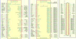
These are the 020 EPROM read back results, minimized with Logic Friday:

Code:
Name     EPROM_READ_T5;
PartNo   ;
Date     ;
Revision ;
Designer ;
Company  ;
Assembly ;
Location ;
Device   virtual;

/* Dedicated input pins */

pin 1   = RAS;       /* Input */
pin 2   = MEMW;      /* Input */
pin 3   = IOR;       /* Input */
pin 4   = AIOW;      /* Input */
pin 5   = Q1;        /* Input */
pin 6   = IO_CS_16;  /* Input */
pin 7   = AEN_1;     /* Input */
pin 8   = AEN_2;     /* Input */
pin 9   = Q4;        /* Input */
pin 11  = FSYS_16;   /* Input */

/* Programmable output pins */

pin 12  = END_CYC;   /* Combinatorial output */
pin 13  = RES_0WS;   /* Input */
pin 14  = DMA_AEN;   /* Combinatorial output */
pin 15  = XA0;       /* Fixed low output w/ output enable */
pin 16  = XBHE;      /* Combinatorial output w/ output enable */
pin 17  = GATE_245;  /* Combinatorial output */
pin 18  = DIR_245;   /* Combinatorial output */
pin 19  = DATA_CONV; /* Combinatorial output */

/* Output equations */

!DATA_CONV =
      !IOR & Q1 & IO_CS_16 & AEN_1 & AEN_2 & !XA0 & !XBHE
    # AIOW & Q1 & IO_CS_16 & AEN_1 & AEN_2 & !XA0 & !XBHE
    # RAS & Q1 & AEN_1 & AEN_2 & !FSYS_16 & !XA0 & !XBHE;

!DIR_245 =
      RAS & MEMW & !AEN_1
    # !MEMW & AEN_1 & AEN_2 & !XBHE
    # AIOW & AEN_1 & AEN_2 & !XBHE;

!GATE_245 =
     !IOR & !AEN_1 & !AEN_2 & FSYS_16 
    # !IOR & !AEN_1 & FSYS_16 & XA0
    # RAS & !AEN_1 & !AEN_2 & FSYS_16
    # RAS & !AEN_1 & FSYS_16 & XA0 

    # !IOR & IO_CS_16 & AEN_1 & AEN_2 & XA0 & !XBHE
    # AIOW & IO_CS_16 & AEN_1 & AEN_2 & XA0 & !XBHE
    # RAS & AEN_1 & AEN_2 & !FSYS_16 & XA0 & !XBHE
    # !MEMW & AEN_1 & AEN_2 & !FSYS_16 & XA0 & !XBHE;

XBHE = AEN_2 & !XA0;

XA0       = 'b'0;

DMA_AEN = AEN_1 & AEN_2;

END_CYC =
      Q4 
    # RAS & !RES_0WS
    # AIOW & !RES_0WS
    # !IOR & Q1 & !IO_CS_16 
    # AIOW & Q1 & !IO_CS_16 
    # RAS & Q1 & FSYS_16;

/* Output enable equations */

!XBHE.oe    =  AEN_1     &  AEN_2;
 XA0.oe     = !AEN_2;

/* End */

And here are the actual source equations which are used to program the GAL chip which read back as above:

Code:
Name     IBM-5170-U87 ;
PartNo   00 ;
Date     26-01-2023 ;
Revision 06 ;
Designer Rodney ;
Company  - ;
Assembly None ;
Location None ;
Device   G16V8A;

/* *************** INPUT PINS *********************/
PIN 15=XA0;
PIN 16=XBHE;
PIN 1=RAS;
PIN 2=MEMW;
PIN 3=IOR;
PIN 4=AIOW;
PIN 5=Q1;
PIN 6=IO_CS_16;
PIN 7=AEN_1;
PIN 8=AEN_2;
PIN 9=Q4;
PIN 11=FSYS_16;
PIN 13=RES_0WS;

/* *************** OUTPUT PINS *********************/
PIN 12=END_CYC;
PIN 14=DMA_AEN;
PIN 17=GATE_245;
PIN 18=DIR_245;
PIN 19=DATA_CONV;

!XBHE.oe    =  DMA_AEN;
 XA0.oe     = !AEN_2;
RES_0WS.oe = 'b'0;

XBHE      =  AEN_2 & !XA0;
XA0       = 'b'0;

DMA_AEN = AEN_1 & AEN_2;

!DATA_CONV =
    AEN_1 & AEN_2 & !FSYS_16 & Q1 & RAS & !XA0 & !XBHE
  # AEN_1 & AEN_2 & !IOR & IO_CS_16 & Q1 & !XA0 & !XBHE
  # AEN_1 & AEN_2 & AIOW & IO_CS_16 & Q1 & !XA0 & !XBHE;

!DIR_245 =
    !AEN_1 & MEMW & RAS
  # AEN_1 & AEN_2 & !MEMW & !XBHE
  # AEN_1 & AEN_2 & AIOW & !XBHE;

!END_CYC =
    FSYS_16 & Q1 & RAS
  # !IOR & !IO_CS_16 & Q1
  # AIOW & !IO_CS_16 & Q1
  # RAS & !RES_0WS
  # AIOW & !RES_0WS
  # Q4;

!GATE_245 =
      RAS & !AEN_1 & FSYS_16 & !XBHE
    # !IOR & !AEN_1 & FSYS_16 & !XBHE
    # !IOR & IO_CS_16 & AEN_1 & AEN_2 & XA0 & !XBHE           
    # AIOW & IO_CS_16 & AEN_1 & AEN_2 & XA0 & !XBHE
    # RAS & AEN_1 & AEN_2 & !FSYS_16 & XA0 & !XBHE
    # !MEMW & AEN_1 & AEN_2 & !FSYS_16 & XA0 & !XBHE;

When looking at the source equation for !GATE_245, we can reason back how the first two terms get distorted by the EPROM read back.

Code:
!GATE_245 =
      RAS & !AEN_1 & FSYS_16 & !XBHE
    # !IOR & !AEN_1 & FSYS_16 & !XBHE
    # !IOR & IO_CS_16 & AEN_1 & AEN_2 & XA0 & !XBHE           
    # AIOW & IO_CS_16 & AEN_1 & AEN_2 & XA0 & !XBHE
    # RAS & AEN_1 & AEN_2 & !FSYS_16 & XA0 & !XBHE
    # !MEMW & AEN_1 & AEN_2 & !FSYS_16 & XA0 & !XBHE;

When DMA occurs, DMA_AEN goes low.
This in turn enables the oe function of XBHE.
XBHE is then generated from:
XBHE = AEN_2 & !XA0;

This leads to the creation of two extra product terms in the EPROM read back result:

Code:
!GATE_245 =
     !IOR & !AEN_1 & !AEN_2 & FSYS_16 
    # !IOR & !AEN_1 & FSYS_16 & XA0
    # RAS & !AEN_1 & !AEN_2 & FSYS_16
    # RAS & !AEN_1 & FSYS_16 & XA0 

    # !IOR & IO_CS_16 & AEN_1 & AEN_2 & XA0 & !XBHE
    # AIOW & IO_CS_16 & AEN_1 & AEN_2 & XA0 & !XBHE
    # RAS & AEN_1 & AEN_2 & !FSYS_16 & XA0 & !XBHE
    # !MEMW & AEN_1 & AEN_2 & !FSYS_16 & XA0 & !XBHE;

When !AEN_2 is true, this enables output XA0 which negates XA0 from being seen as part of the product term, so XA0 disappears in those EPROM results which forms a separate product term in the equation results. This occurs twice, once in the "!IOR" term and once in the "RAS" term.
When AEN_2 is true, this takes XA0 again from the read input, thus showing up in the equation, because it was analysed as being a part of that product term.

Why do we see XA0 "showing up" and not !XBHE as per the original equation?
Because !XBHE is generated from !(AEN_2 & !XA0).
AEN_2 is true, so it equals 1, and we are left with !XBHE = !(!XA0) = XA0 being substituted in the minimized EPROM read result.
Somehow, I believe that !XBHE gets minimized away from those product terms, I am still somewhat unclear on the automated process of how this happens since many minimized lines would be involved, however I can at least observe the resulting equation and attempt to form a theoretical explanation for this.

This is my theory which is also indicated by the identical EPROM read result as U87.
So the equations at least produce the exact matching result to create the additional result terms.

I don't exclude that there are other hidden things, though I am not seeing those at first glance.
The additional effects occur when DMA happens which is only happening in the first two product terms of the "original equation" for !GATE_245.
The last 4 of the 6 terms are non-DMA situations involving the CPU.
There is some DMA happening in DIR_245 but the equation do not involve the inputs XA0 and/or XBHE since they only detect the direction of the conversion transceiver.

Since we have analysed what happens to the related DMA lines in GATE_245, this would suggest that possibly no more "surprises" would be hiding inside U87.

I attached revision 6 of the GAL equations for U87, as well as the 27C020 read back bin file so you can test with this Johann.

I should note that both revision 5 and revision 6 function perfectly, but as you mentioned, it is also nice to actually observe the identical logic in the read back result itself.
In fact, during my tests I also believed that !XBHE is actually not needed at all in the first two terms of !GATE_245, which was proven in a perfectly functioning 5170, however for correctness let's keep to the "matching" version 6, which is also my preference and why I spent the time on it today after all.

I was entertaining a final thought while doing this work. Now we may have the fully original equations as far as known to us, then how could one arrive at that conclusion in software?
That seems to be incredibly complicated because combinations of output logic apply differently to the measurements by EPROM reads. So how to detect for this in software?
Quite possibly only a human person could attempt to see patterns and use logical reasoning to predict the original equations which were distorted.
How would it be possible to construct and predict the whole "system" as it were, from the EPROM readings alone?
To me this looks like an extremely difficult problem.
 

Attachments

  • U87_logic_Rev_06.zip
    10.4 KB · Views: 3
Also, I was thrown off in the beginning of my work by seeing "!AEN_1 & !AEN_2" in the product terms for !GATE_245, which situation would constitute bus master DMA on an ISA card.
That was at the beginning when I was not considering XA0 and XBHE possibly being outputs and the consequences of this.
So I tried to explain this by reasoning a situation where the DMA bus master on the card would communicate with an 8 bit device or 8 bit mode RAM.
However when I reconsider this thought, it seems not very likely since an 8 bit device would not be involved in a bus master operation since this has no advantage performance-wise.
The 8 bit floppy drive controller may be present on a card in most configurations, however it's still controlled by BIOS routines which involve DMA controller 1 on the mainboard.

I have verified the EPROM read results for both U87 and the Rev 6 GAL recreation of U87 and they are indeed 100% matching in the reduced logic.

Thank you Johann for putting me on the trace of this matter by doing an analysis of the GAL.
When I noticed the missing MEMW term from the EPROM read I just still felt unsatisfied with the source code after all.
I couldn't help but look at it again more closely. When it was originally programmed, it should be possible somehow.
As it turns out, !GATE_245 even has only 6 product terms originally, well within the capability of the PAL.

I want to go for authentic circuits which reflect at least the "secret sauce" concepts of the original IBM creators to be preserved in the new design.
Functional expansions, improvements and upgrades I am completely fine with on the other hand as long as they feel like a reasonable match with the system.
 
Last edited:
Hi Johann,

I suddenly got a thought. Perhaps it would be a good idea to first generate an intermediate merge file after discovering a PIN.oe function.
The merge file can initially return to all the detected logic states created in the initial step, so before minimization.
This creates a base point of logic where the changed states for the modified inputs can be injected.

I think when each PIN.oe is true, the logic evaluation should replace the input PIN by the equation which it represented during PIN.oe is true, as detected in the "first pass" minimization step.

Possibly this injection of states into the initial data from the EPROM read can create the actual situation inside the chip by substituting the original pin name with the replacement logic in all the terms, since it is literally replaced by the different equations for that pin during those PIN.oe is true conditions.

Looking at the U87 example, we can see that running such a second pass "post processing" step could result in another simplification of the final minimized equation set.

So this would require some form of "search and replace" routine to apply the "input to output" replacements in all the initial step product terms.

After this you could re-apply the usual minimizations.
You could use our U87 as a means of verification for this procedure to see how it turns out.

I have no idea how involved this would become to program, I am only thinking out "loud" here and sharing my thoughts.
Perhaps such a procedure could also yield more information about U130 which is definitely also carrying several feedbacks to generate more complex types of logic parts.

I have a suggestion, if some time in the future I do some work on the SNES copybox, we could test out the procedures to see how they apply. I am not getting into a fight with Nintendo so I can't publish anything but I can at least test the software out on some chips just to have a look. Though they are all GAL chips and similar so perhaps not suitable. The DRAM control will probably occupy half the logic and can be discarded. Then is left some output port logic and FDC control interfacing which is really predictable from the FDC chip datasheet.

And maybe I have some more PALs from various arcade PCBs I have in my storage here. I just checked a Tiger Heli PCB which I play sometimes with my daughters and it contains at least a PAL16R4, so not an ideal specimen anyway. But I may turn up some PAL16L8 parts somewhere which could be interesting subjects to test these methods on. I could do the PALs on the ARC mainboard for example but it requires a lot of time to trace out the connections so I can get the right names. I don't want to go off on a tangent right now because I prefer to steam ahead on our project we are working on here.
 
Last edited:
I'm currently working on the design of the first CPLD in Quartus 13.0 as lowen advised me, it takes some getting used to the schematic drawing interface.
I am using the device EPM7128SLC84-10 for now in the settings in order to get started, I think it should be compatible with the ATF1508AS which will actually be used.

It makes no sense to use smaller CPLDs in this system so I am going to use at least 84 pin chips.

I made a section in KiCad for the logic which I am moving into the CPLD.
After getting the CPLD done, I will split off that section into a separate backup KiCad schematic and draw in the new CPLD based part into the new design schematic.
So I will be doing double checking on the separate KiCad schematic later to verify the CPLD before designing the PCB.

Since the CPLD also supports D Flipflops, I will move all of these into CPLDs as well.
A clocked part should not cause any problems due to the much higher speed of the CPLD, at least I hope so.

Also, a faster propagation in decoding logic gates should have a positive influence on the system stability.
The most problems I have experienced in the past are due to propagation which was too slow.

I will be using at least two CPLD chips of 84 pin PLCC package which can fit into through-hole PLCC sockets.
As things are looking right now, these will be the ICs featured on the mainboard:
- 5170 System controller
- Memory and I/O controller

Since the elaborate logic inside the PALs is forcing me to look into CPLD technology anyway to be able to even fit everything on the mainboard, I might as well benefit even more from the advantages of CPLDs and at least free up PCB space. It is my hope that the higher logic speed of the CPLDs would allow even higher clock speeds for a CPU later on in future revisions.
I have visions of playing Doom on a 486 SLC chip or emulated CPU with some higher clock speeds, and possibly being able to run Windows 95 on later revisions.

I don't like chipsets, not because of the technology but because of the lack of documentation of the logic making it impossible to make new chips. It's a dead-end solution which when the chips are defective will render systems unusable and basically become scrap boards for parts usage. That is my biggest dislike of chipsets. What I am doing now of course has some overlap with what chipset makers did, with the one important difference, I will share the technology contained in the chips for the open source designs, of course under the terms of hobby and educational usage and preservation of the historic technology only.

I have looked at VHDL for defining the logic where I have studied some code examples which is nice to see the logic in that method, but I will not be doing this at this moment.
It is simply too involved to combine this with my project, I do plan to get the mainboard made this year, and the sooner, the better.
I bought a book years ago but this 700+ page book focuses directly on more complex designs, which is understandable but not so suitable for this particular situation.

So I will be using the schematic design method for now. Perhaps later I can see VHDL representations and learn from those to see if that would be a future option.

As I understand it now, there is at least a feature to create signal names in the schematic entry, so I can keep a better overview in the design.
I watched some example video's which describe the process of drawing a line from a logic gate and while the line is selected typing the signal name which creates a net that connects to all other signals carrying the same net.

Quartus can't directly program the Atmel parts, but is a much better design environment than the Atmel-supported WinCUPL. You CAN get Atmel's ProChip designer, but it's commercial software and relatively pricey. But you CAN generate the POF files used to program the Altera MAX7000S parts and then convert, using POF2JED, into files ATMISP, the Atmel programmer, can then program the Atmel parts.
lowen, I wonder, could I ask you some questions in case I can't find something by studying tutorials?

When I connect two logic elements in the schematic design using signal names which I type at the gates, after I save the schematic and run the RTL viewer, the pins appear as connected. So it appears to be in order to draw schematics in this way.
I also saw that certain buffer types are not possible on the device, but I found other more simple tri-state buffer types which are supported apparently.

I will update here if I find more useful basic stuff for using Quartus that I can share.
 
Last edited:
Sorry, I didn't have much time this weekend, so only a small update...

One of the questions was, why PA.EXE and pa.py disagree about XBHE.

PA.EXE says:
XBHE = AEN_2 & !XA0

pa.py says:
XBHE = !AEN_1 & AEN_2 & !XA0

PA.EXE and pa.py agree on OE:
XBHE.oe = !AEN_1 & !AEN_2
# AEN_1 & !AEN_2
# !AEN_1 & AEN_2

Without source code, I cannot say how PA.EXE infers that, but I know how pa.py works:
- First step: It sees that changing AEN1 changes XBHE, so it records this information
- Second step: It checks all combination of input pins for which "XBHE = 1"; and it sees that this is only the case when AEN = 0

You could also rewrite the PA.EXE equation to:
XBHE = !AEN_1 & AEN_2 & !XA0
# AEN_1 & AEN_2 & !XA0
But for the second product "AEN_1 & AEN_2", XBHE.oe is false, so that the XBHE result is irrelevant ("don't care").

In other words, PA.EXE and pa.py equation is (mathematically) equivalent. I have however no idea if PA.EXE has some clever way to perform this simplification or if it has a bug...
 
You could also rewrite the PA.EXE equation to:
But for the second product "AEN_1 & AEN_2", XBHE.oe is false, so that the XBHE result is irrelevant ("don't care").
Hi Johann,

It's nice to hear from you.

Our discussions are really valuable to me. Your theory is illuminating indeed, I had not looked into this matter deeply yet, so thanks for looking at it.

The analysis of outputs as a product of inputs does contain some chance of missing some information in the results because the information cannot be derived from the states of signals only, when OE functions get involved. It's another example of byproducts being created in the analysis.

Just like in the case of !GATE_245 where the analysis is producing extra product terms due to observing the resulting states of the whole logic when oe controlled output pins get activated.

I think it's not too important in this case of AEN_1.

In case of the 5170, we are working to obtain purity of the original data conversion PAL as made by IBM because it's our purpose for historical reasons to chase the complete original concept.

In other cases the analysis of a PAL is usually done for the primary purpose of getting a functional chip to repair or historically reproduce a machine which would otherwise be lost or would become a dead scrap parts board. Many machines are arguably too precious to just discard or strip for parts. And, personally, I don't like the thought that some IBM mainboard would never be used again just because of a single missing or dead component which is irreplacable. Thanks to the work in this thread, now it isn't.

Since when AEN_1 is also true, XBHE is not generated by the PAL anyway, as you pointed out, I will leave this signal out of the equation.
IBM would surely have known this condition to be invalid for the operation of DMA so we can argue that they most likely did not program that in, in the first place.

It's going well working with Quartus. I am moving a lot of logic into the first CPLD.
After I get everything into the CPLD, I will evaluate if there are any pins still available for other circuits.
Then I can proceed to focus on integrating the chip into the new mainboard schematic and checking the signal flow of the whole chip as it is integrated into the system to be correct.

I am thinking of future projects where I would really love to see some work done on the 8237 DMA controller, 8259 interrupt controller, 8254 timer chip and the system controller chips 8284, 82284, 82288 in FPGA or CPLD reproduction versions. This would free new builders from needing to obtain old parts just to be able to reproduce a new AT PC to be able to enjoy the experience.

If anyone knows some projects where this type of work was done, I would really appreciate a message about this.
Probably after my first prototype for this project I will take a look at moving the 8284, 82284 and 82288 into a CPLD.
I could try to create them in programmable logic and test them on the 5170.
Anyway, those are just a few thoughts when considering preservation of the 286 AT system.
 
I am looking at the system controller CPLD design and I have studied some PDF documentation from Atmel about the 15xx CPLD family.

I see a few important points worth mentioning here:

- the Atmel 1508AS is pin-compatible with the Altera MAX7000S, so it looks like the pin assignments made in Quartus can be used for programming the 1508AS.
- there are some "global" clock, clock enable, clear and OE pins which can be used to control flipflops in the design.
- there are 16 pins used for power and ground
- there are 4 pins used for JTAG programming of the CPLD if we want to keep in circuit programming which otherwise would require special programmers to "reset" the chip design when JTAG pins are repurposed.

An 84 pin CPLD subsequently would yield 64 usable pins. Which is actually not that much in our application of an AT system.
We do have some clock signals entering into the CPLD design, however these are far from having a "global" connection nature to use for flipflops, nor is there any bus-wide type action going on which could benefit from a global clear etc. I did add the fastest clock inputs to the global clock pins, maybe this would be better because at least the fastest clocks around 16Mhz arrive directly in all areas of the CPLD and at least won't need to travel unnecessarily through more logic inside the chip I believe.

So I am not going to use any global function in the CPLD, I assume to be rather pointless.
This is my first CPLD design so I will see what happens regarding the timing of the system. It functionally replicates the 5170 circuits including U87 so using a CPLD should at least provide some advantages in the propagation delays compared to regular F and ALS logic family circuits of the 5170 combined with the U87 logic. And it adds the advantage to reduce the board area which leaves more space available to use for onboard interfaces etc. I am hoping that we could achieve the typical system stability as seen in chipset systems while keeping close to the 5170 concept where it counts for the project purpose, and maintaining the open source nature as intended for this hobby/educational project.

I am going to separate the clock generation to create certain clock paths to be CPU/conversion involved, which we may want to experiment with in the future, and fixed clock generation separately for the 8237 DMA controllers and supporting logic for DMA functional control, 8042 keyboard controller and 8254 timer chip, just as I have done before with the XT design. This way, any clock experimentation will not crash these chips which can't and should not exceed their specified clock speeds for various reasons or the system won't run stable for sure.

Of course, in the case of the CPU that's another matter and I will be testing to see how far this may be stretched a little bit using a faster spec 286 processor, and of course in future steps as I am planning to take, using the 486SLC chip. The faster the CPU runs, the more the memory speeds will get involved in limiting the possible stable clock speeds. I have many more design steps planned after these, including to look at faster bus types. After the 286 design is fully done and tested and I see no more improvements possible that I want to do, I will more on to a faster 16 bit CPU such as the 486SLC. Another possible path would be emulation of faster 16 bit configurations, if there is any current open source project to be found which would support doing that.

I will use the OSC, 286_CLK and a "16M" input as separate clock inputs so I can reprogram the CPLD to generate any clock speeds in any necessary combinations on the clock outputs. The 286_CLK could be increased later on and let's see what happens then.

The 8237 I will test to run at 4.77 Mhz derived from OSC which I think is a best speed for these chips to run completely stable, as this speed is already tested successfully in a 8Mhz turbo XT design. We will have to see after testing if the timing specs of the system circuits in this project are sufficient to facilitate this DMA clock speed since IBM originally designed the system to run at 4Mhz DMA clock. Every speed increase is of course welcome if the system can run stable. The timer will run at the normal system timer clock speed of 1.19Mhz, and the keyboard controller runs at 8Mhz.
If there is any problem, using the CPLD I can change the DMA controllers to run at 4Mhz if needed. Using 3 clock inputs and using separate clock circuits gives all the flexibility which could be necessary in this project.

I was not able to include the coprocessor control because of running out of pins in the package, so I will try to include it into the "decoder" CPLD design, which is up next.
The decoder CPLD will focus on I/O and memory decoding primarily to obtain the best use of the chip and other things I will add in if pins are available for that.

By the way, it's funny, or rather cool, that quartus is so smart to detect and report the "combinational loop" as designed by IBM engineers in the DMA functional control circuits.
After stripping out the refresh stuff this is what I was left with from the functional logic which serves to control DMA.
 
Good news: pa.py now outputs the same equations as PA.EXE, including "XBHE = AEN_2 & !XA0" instead of "XBHE = !AEN_1 & AEN_2 & !XA0". I've written a detailed explanation into the source code and won't repeat it here. Moreover, pete.py now outputs the same equations as PA.EXE + logic Friday.

And, I might have found an algorithm to even generate the more simplified 6-term ~GATE_245 instead of the 8-term, which until now was only found by NI (natural intelligence, aka Rodney ;-)).

Rodney, my respect for your work to find the 6-term solution and fully matching the PAL behavior - not sure if I would have found it myself! Below is based on your work, I just needed to rethink and reformulate it so that I'm able to hopefully turn this into Python code.

So, as outlined by Rodney earlier, the terms (part of ~GATE_245)
Code:
    ~AEN_1 &           FSYS_16 &                      RAS &       XA0
  | ~AEN_1 & ~AEN_2 &  FSYS_16 &                      RAS
  | ~AEN_1 &           FSYS_16 &                                  XA0 & ~IOR
  | ~AEN_1 & ~AEN_2 &  FSYS_16 &                                        ~IOR
can be simplified to:
Code:
    ~AEN_1 &           FSYS_16 &                      RAS                    & ~XBHE
  | ~AEN_1 &           FSYS_16 &                                      & ~IOR & ~XBHE

or, using just one half of it, to have a smaller example:
Code:
    ~AEN_1 &           FSYS_16 &                      RAS &       XA0
  | ~AEN_1 & ~AEN_2 &  FSYS_16 &                      RAS
can be simplified to:
Code:
    ~AEN_1             FSYS_16 &                      RAS                    & ~XBHE

Mathematical evidence, why both is equivalent:
XBHE = AEN_2 & ~XA0 => ~XBHE = ~AEN2 | XA0
so the one line in the last code snippet can be replaced by the previous two lines, one time replacing "~XBHE" by "~AEN2" and one time replacing "~XBHE" by "XA0".
 
Mathematical evidence, why both is equivalent:
XBHE = AEN_2 & ~XA0 => ~XBHE = ~AEN2 | XA0

Hi Johann, great discovery and explanation, that's the final clue making sense of what happened, you found it that it's actually DeMorgan's from AND to OR that can reproduce it! I just had another look at my earlier post after reading your update, and then I also noticed it, and I was writing into my notes the same things as you just explained!

It makes sense that analysis with PA.EXE did not manage to substitute these terms before because the PA.EXE source code is not equipped to do this, as we now know.
If only it could have, looking back, that would have saved me so much work and sleepless nights trying to figure out how to reduce the terms. On the other hand this work has shown us something important and evidently a clear limitation of PA.EXE.

But now you have uncovered the mathematical reason for it, I see what you mean that this can lead to an actual discovery of the substitution in your scripting work, which to me is really pretty amazing to achieve this in programming! I hope this feature could become useful for discovering similar functions in future PAL analysis! That could save some potential future headaches. Besides a possible "storage" feedback, this OE function is really able to complicate things if applied by the original programmer. Or possibly some type of OE function could actually produce a storage feedback, I don't exclude that it would be possible somehow.

Maybe your new code could yield more information from the U130 data. Though I have left it out of my first CPLD due to pin limits of that CPLD, I want to include it later on into a final design of course.

Who knows, if we could discover an actual latch function, it could be possible to predict this type of PAL usage as well from the read results.
Like a similar situation, when knowing the phenomenon, it might be explained with mathematical reasoning.
But maybe I'm too optimistic about this point, it seems even more complicated, but after this experience, not impossible though, great work!

For now, I will focus on progressing the integration work necessary to get us to a complete working AT system.
The first CPLD is full, so I will start working on the second one. I don't want to switch to much larger ICs because it will probably mean that it's not available in PLCC package anymore which I do want to keep so we can solder it in through hole using a socket.

As soon as I have the core logic for the 5170 mainboard ready, I will proceed to integrate the usual interfaces of an AT ISA system into the mainboard design, and after having done all the verifications and checks of the 5170 derived core logic that I'm planning to do, I can start working on the actual PCB layout. It is my plan to do a two layer design if possible.
 
It turns out that due to the number of pins needed, there will be 3 CPLDs necessary to implement the complete AT system:
- System decoder
- Memory decoder
- IO decoder

By splitting the logic in three sections, it becomes possible to create full decoding for everything that we want to add onboard and possibly even some more.

The system controller contains:
- clock dividers, separated paths for fixed and "to be possibly experimented with" clocks
- DMA control and CPU READY handshaking signals
- wait state logic
- CPU shut down control
- 8 to 16 bit conversion control, CPU cycle extension during conversions
- X bus IO space decoding
As discussed, we are paying care to include the original IBM secret sauce logic, including the contents of U87 as we believe to be 100% accurate and verified.

For now I have divided the memory map as follows:
Code:
000000 - 09FFFF    640KB conventional RAM      16 bit mode
0C8000 - 0D0000    32KB of option ROM space    8 bit mode
0D0000 - 0EFFFF    128KB UMB RAM               16 bit mode
0F0000 - 0FFFFF    2 BIOS ROMs                 16 bit mode
100000 - 8FFFFF    8MB of XMS RAM              16 bit mode

In future systems when it's possible to use a 486SLC CPU, I will look at using more RAM after studying this CPU separately and in detail.
For example when using windows 95 or perhaps some linux form as boot options next to DOS, more RAM will become more useful and advantageous.

Controlling more RAM will require more pins from the memory decoder for which I will look at splitting the high and low byte selects to some method externally from the CPLD.
For the first prototype I have created separate high and low byte RAM chip selects in the CPLD just to simplify controlling the memory PCB and for a first test of the whole system.

I am going to use a different structure in the memory decoder from IBM's method. IBM first creates the decoding from the CPU address lines and then runs the finished CS signals through a GATE_ALE(combined CPU active address valid and CPU in hold state for DMA controller or bus master) latch to make sure no undefined address states end up on the chip selects. My method is slightly different, I will first "clean up" the source address lines from the CPU using the GATE_ALE latching, and then run those through the decoding logic which directly creates the chip select lines. The memory selected will become accessible through the memory read and write signals. This is an approach which appeals more to me.

In the IO decoder which is up next, I will decode all of the IO devices onboard, including the typical AT interfaces. This will reduce the onboard logic area needed for these and will help to include more IO on the mainboard itself. If there are some spare pins left on the IO decoder I will create a few headers which can be used to add more IO and simplify new ISA PCBs by integrating the decoding logic for them on the mainboard decoder itself. This feature is purely optional and can be used as a flexible design option if so desired by builders, and will give us even more usage from the presence of CPLDs on the mainboard.

I will provide JTAG headers for in circuit programming. Also I plan to add an ISP jumper which keeps the system in reset while powering all the CPLDs during programming. This can make sure the system is not doing anything at those times.
 
Rodney, I think I found a way to let sympy simplify the !GATE_245 equation to 6 terms:
Code:
!GATE_245 = 
    FSYS_16 & RAS & !AEN_1 & !XBHE
  # FSYS_16 & !AEN_1 & !IOR & !XBHE
  # AEN_1 & IO_CS_16 & XA0 & !IOR & !XBHE
  # AEN_1 & AIOW & IO_CS_16 & XA0 & !XBHE
  # AEN_1 & RAS & XA0 & !FSYS_16 & !XBHE
  # AEN_1 & XA0 & !FSYS_16 & !MEMW & !XBHE

These look similar to yours, but do not have "AEN_2" in the lower four terms. I *think* this might be ok, because XBHE==0 already satisfies AEN_2==1 (because XA0==1), but I'm not 100% sure. So before I explain how I did it and it turns out I did it wrongly, would you be so kind and try out if the EPROM readout is identical with my !GATE_245 equation?
 
Hi Johann,

I am not sure about the exact reason for this to happen in your result where AEN_2 disappeared, though that is very interesting.

I am certainly not excluding the possibility that the original equations are in fact even still different from the previous assumptions because everything we do is only possible as a result of analyzing all the logic states which are known. More possibilities still could have remained hidden up to now where certain inputs are influencing eachother. More variations could be in fact logically equivalent as seen from the analysis results.

I will test your new equations on the 5170 and read back the states using my programmer and EPROM/resistor adapter.
 
Hi Johann,

Exciting news!

Here is the result from PA.EXE analysing the 27C020 EPROM with resistor adapter read:

Code:
!GATE_245 =
      RAS & !AEN_1 & !AEN_2 & FSYS_16 
    # !IOR & !AEN_1 & !AEN_2 & FSYS_16 
    # RAS & !AEN_1 & FSYS_16 & XA0 
    # !IOR & !AEN_1 & FSYS_16 & XA0 
    # !IOR & IO_CS_16 & AEN_1 & AEN_2 & XA0 & !XBHE
    # AIOW & IO_CS_16 & AEN_1 & AEN_2 & XA0 & !XBHE
    # RAS & AEN_1 & AEN_2 & !FSYS_16 & XA0 & !XBHE
    # !MEMW & AEN_1 & AEN_2 & !FSYS_16 & XA0 & !XBHE;

Which is 100% identical with my previous U87 PA.EXE results.

I have tested the GAL on the 5170 and I am able to format a floppy disk and sound is working through a DMA channel.

So apparently you have discovered something new, my congratulations!

I will save this set of equations as version 7 of the U87 replacement and keep testing with these from now on.
I also included the compilation results from WinCupl in the attachment.

Simply amazing that you have achieved this result with your python programming work Johann!
 

Attachments

  • GAL test results for Johann.zip
    15.3 KB · Views: 1
If anyone is curious about my progress here is a screenshot of the system controller and memory decoder CPLDs.

I am currently working on the IO decoder which will decode all the onboard device IO ports.

I will feature some LED indicators next to the CPLDs on the mainboard which signal their activity.
 

Attachments

  • CPLDs.png
    CPLDs.png
    78.7 KB · Views: 8
Hi Johann,

Such a coincidence, I was checking something on a ISA adapter card which features an AT IDE port and floppy drive controller, and what did they use for the decoding? A PAL16L8!

So I have read it out and used PA.EXE on it, the information is really simple compared to U87, however I am doubting it is 100% accurate.
So I attach the EPROM read here.

I know you are really busy with your work, so I just leave this message here for you in case you have some time to look at it later.

A little information about the board:

Code:
PAL 16L8:

1    SA0
2    SA1
3    SA2
4    SA3
5    SA4
6    SA5
7    SA6
8    SA7
9    SA8
11    SA9
12    /FDC_LDOR
13    /FDC_DC
14    AEN
15    /FDC_LDCR
16    /IDE_CS1
17    /FDC_CS
18    74LS125 PIN9    10=PULLUP 11=PULLUP TO JUMPER RELATED TO IDE PIN 31
19    /IDE_CS0

From PA.EXE I am getting the following:

Code:
Name     EPROM_READ_27C020;
PartNo   ;
Date     ;
Revision ;
Designer ;
Company  ;
Assembly ;
Location ;
Device   virtual;

/* Dedicated input pins */

pin 1   = SA0;       /* Input */
pin 2   = SA1;       /* Input */
pin 3   = SA2;       /* Input */
pin 4   = SA3;       /* Input */
pin 5   = SA4;       /* Input */
pin 6   = SA5;       /* Input */
pin 7   = SA6;       /* Input */
pin 8   = SA7;       /* Input */
pin 9   = SA8;       /* Input */
pin 11  = SA9;       /* Input */

/* Programmable output pins */

pin 12  = FDC_LDORn; /* Combinatorial output */
pin 13  = FDC_DCn;   /* Input */
pin 14  = AEN;       /* Input */
pin 15  = FDC_LDCRn; /* Combinatorial output */
pin 16  = IDE_CS1n;  /* Combinatorial output */
pin 17  = FDC_CSn;   /* Combinatorial output */
pin 18  = LSPIN9;    /* Combinatorial output */
pin 19  = IDE_CS0n;  /* Combinatorial output */

/* Output equations */

!IDE_CS0n  = !SA3       &  SA4       &  SA5       &  SA6       &  SA7       &  SA8       & !SA9       & !AEN;
!IDE_CS1n  =  SA1       &  SA2       & !SA3       &  SA4       &  SA5       &  SA6       &  SA7       &  SA8       &  SA9       & !AEN;
!LSPIN9    =  FDC_DCn;
!FDC_CSn   = !SA1       &  SA2       & !SA3       &  SA4       &  SA5       &  SA6       &  SA7       &  SA8       &  SA9       & !AEN;
!FDC_LDCRn =  SA0       &  SA1       &  SA2       & !SA3       &  SA4       &  SA5       &  SA6       &  SA7       &  SA8       &  SA9       & !AEN;
!FDC_LDORn = !SA0       &  SA1       & !SA2       & !SA3       &  SA4       &  SA5       &  SA6       &  SA7       &  SA8       &  SA9       & !AEN;

/* End */

It's highly doubtful that the PAL would merely pass through the input FDC_DC to inverted output LSPIN9, it seems too simple and would not serve a logical purpose. Though I am not excluding it to be simple either.

I tried to beep out the PCB which I have done partially, I will continue that later on. The LSPIN9 goes to a 74LS125 port which passes on to what looks like a unpopulated jumper. Though I can't be sure because the silkscreen is really limited on the PCB to only very few things.

All of the output pins are negative active.

Here is the information in a table form copied directly from my overview spreadsheet of decoding ports:
/IDE1_CS00111110IIIII1F0
/IDE1_CS11111110113F6
BA9BA8BA7BA6BA5BA4BA3BA2BA1BA0/BIOR/BIOW
/FDC_LDOR (AT)11111100103F2
/FDC_CS (AT)111111010F3F4/3F5
/FDC_LDCR (AT)11111101113F7

The capital letters in the table like "I" or "F" mean that the interface or chip is decoding that signal itself.
Where you see the 1 or 0 noted, this is decoded by the decoder PAL. Sometimes both apply, like for example the FDC chip also looks at A0 itself.
 

Attachments

  • EPROM_READ_27C020.zip
    1.2 KB · Views: 2
  • Img_3134.jpg
    Img_3134.jpg
    129.3 KB · Views: 8
Last edited:
So, here comes the explanation why we were not yet able to get the simplified U87 equations without some manual "tuning"...

First of all, from checking the whole "EPROM dump" and comparing input to output bits in a rather brute-force way, we know that the following 10 pins can impact the GATE_245 output:
Code:
RAS, MEMW, IOR, AIOW, IO_CS_16, AEN_1, AEN_2, FSYS_16, XA0, XBHE

Furthermore, let's look at one product term of !GATE_245:
Code:
RAS & !AEN_1 & FSYS_16 & !XBHE

In other words, the following 4 conditions are sufficient for GATE_245==0
Code:
RAS==1
AEN_1==0
FSYS_16==1
XBHE==0

So, 4 pin conditions are sufficient for GATE_245, and the other 6 are irrelevant in this situation. We would expect that permuting the 6 other pins would always result in low output, right? And a boolean algebra simplifier would recognize that these 6 pins can be removed from the equation, right? Wrong!!!

Looking at the "EPROM dump", we get:
Code:
 RAS       ~MEMW      ~IOR       ~AIOW      ~IO_CS_16  ~AEN_1     ~AEN_2      FSYS_16   ~XA0       ~XBHE      -> low
 RAS        MEMW      ~IOR       ~AIOW      ~IO_CS_16  ~AEN_1     ~AEN_2      FSYS_16   ~XA0       ~XBHE      -> low
 RAS       ~MEMW       IOR       ~AIOW      ~IO_CS_16  ~AEN_1     ~AEN_2      FSYS_16   ~XA0       ~XBHE      -> low
 RAS        MEMW       IOR       ~AIOW      ~IO_CS_16  ~AEN_1     ~AEN_2      FSYS_16   ~XA0       ~XBHE      -> low
 RAS       ~MEMW      ~IOR        AIOW      ~IO_CS_16  ~AEN_1     ~AEN_2      FSYS_16   ~XA0       ~XBHE      -> low
 RAS        MEMW      ~IOR        AIOW      ~IO_CS_16  ~AEN_1     ~AEN_2      FSYS_16   ~XA0       ~XBHE      -> low
 RAS       ~MEMW       IOR        AIOW      ~IO_CS_16  ~AEN_1     ~AEN_2      FSYS_16   ~XA0       ~XBHE      -> low
 RAS        MEMW       IOR        AIOW      ~IO_CS_16  ~AEN_1     ~AEN_2      FSYS_16   ~XA0       ~XBHE      -> low
 RAS       ~MEMW      ~IOR       ~AIOW       IO_CS_16  ~AEN_1     ~AEN_2      FSYS_16   ~XA0       ~XBHE      -> low
 RAS        MEMW      ~IOR       ~AIOW       IO_CS_16  ~AEN_1     ~AEN_2      FSYS_16   ~XA0       ~XBHE      -> low
 RAS       ~MEMW       IOR       ~AIOW       IO_CS_16  ~AEN_1     ~AEN_2      FSYS_16   ~XA0       ~XBHE      -> low
 RAS        MEMW       IOR       ~AIOW       IO_CS_16  ~AEN_1     ~AEN_2      FSYS_16   ~XA0       ~XBHE      -> low
 RAS       ~MEMW      ~IOR        AIOW       IO_CS_16  ~AEN_1     ~AEN_2      FSYS_16   ~XA0       ~XBHE      -> low
 RAS        MEMW      ~IOR        AIOW       IO_CS_16  ~AEN_1     ~AEN_2      FSYS_16   ~XA0       ~XBHE      -> low
 RAS       ~MEMW       IOR        AIOW       IO_CS_16  ~AEN_1     ~AEN_2      FSYS_16   ~XA0       ~XBHE      -> low
 RAS        MEMW       IOR        AIOW       IO_CS_16  ~AEN_1     ~AEN_2      FSYS_16   ~XA0       ~XBHE      -> low
 RAS       ~MEMW      ~IOR       ~AIOW      ~IO_CS_16  ~AEN_1      AEN_2      FSYS_16   ~XA0       ~XBHE      -> high
 RAS        MEMW      ~IOR       ~AIOW      ~IO_CS_16  ~AEN_1      AEN_2      FSYS_16   ~XA0       ~XBHE      -> high
 RAS       ~MEMW       IOR       ~AIOW      ~IO_CS_16  ~AEN_1      AEN_2      FSYS_16   ~XA0       ~XBHE      -> high
 RAS        MEMW       IOR       ~AIOW      ~IO_CS_16  ~AEN_1      AEN_2      FSYS_16   ~XA0       ~XBHE      -> high
 RAS       ~MEMW      ~IOR        AIOW      ~IO_CS_16  ~AEN_1      AEN_2      FSYS_16   ~XA0       ~XBHE      -> high
 RAS        MEMW      ~IOR        AIOW      ~IO_CS_16  ~AEN_1      AEN_2      FSYS_16   ~XA0       ~XBHE      -> high
 RAS       ~MEMW       IOR        AIOW      ~IO_CS_16  ~AEN_1      AEN_2      FSYS_16   ~XA0       ~XBHE      -> high
 RAS        MEMW       IOR        AIOW      ~IO_CS_16  ~AEN_1      AEN_2      FSYS_16   ~XA0       ~XBHE      -> high
 RAS       ~MEMW      ~IOR       ~AIOW       IO_CS_16  ~AEN_1      AEN_2      FSYS_16   ~XA0       ~XBHE      -> high
 RAS        MEMW      ~IOR       ~AIOW       IO_CS_16  ~AEN_1      AEN_2      FSYS_16   ~XA0       ~XBHE      -> high
 RAS       ~MEMW       IOR       ~AIOW       IO_CS_16  ~AEN_1      AEN_2      FSYS_16   ~XA0       ~XBHE      -> high
 RAS        MEMW       IOR       ~AIOW       IO_CS_16  ~AEN_1      AEN_2      FSYS_16   ~XA0       ~XBHE      -> high
 RAS       ~MEMW      ~IOR        AIOW       IO_CS_16  ~AEN_1      AEN_2      FSYS_16   ~XA0       ~XBHE      -> high
 RAS        MEMW      ~IOR        AIOW       IO_CS_16  ~AEN_1      AEN_2      FSYS_16   ~XA0       ~XBHE      -> high
 RAS       ~MEMW       IOR        AIOW       IO_CS_16  ~AEN_1      AEN_2      FSYS_16   ~XA0       ~XBHE      -> high
 RAS        MEMW       IOR        AIOW       IO_CS_16  ~AEN_1      AEN_2      FSYS_16   ~XA0       ~XBHE      -> high
 RAS       ~MEMW      ~IOR       ~AIOW      ~IO_CS_16  ~AEN_1     ~AEN_2      FSYS_16    XA0       ~XBHE      -> low
 RAS        MEMW      ~IOR       ~AIOW      ~IO_CS_16  ~AEN_1     ~AEN_2      FSYS_16    XA0       ~XBHE      -> low
 RAS       ~MEMW       IOR       ~AIOW      ~IO_CS_16  ~AEN_1     ~AEN_2      FSYS_16    XA0       ~XBHE      -> low
 RAS        MEMW       IOR       ~AIOW      ~IO_CS_16  ~AEN_1     ~AEN_2      FSYS_16    XA0       ~XBHE      -> low
 RAS       ~MEMW      ~IOR        AIOW      ~IO_CS_16  ~AEN_1     ~AEN_2      FSYS_16    XA0       ~XBHE      -> low
 RAS        MEMW      ~IOR        AIOW      ~IO_CS_16  ~AEN_1     ~AEN_2      FSYS_16    XA0       ~XBHE      -> low
 RAS       ~MEMW       IOR        AIOW      ~IO_CS_16  ~AEN_1     ~AEN_2      FSYS_16    XA0       ~XBHE      -> low
 RAS        MEMW       IOR        AIOW      ~IO_CS_16  ~AEN_1     ~AEN_2      FSYS_16    XA0       ~XBHE      -> low
 RAS       ~MEMW      ~IOR       ~AIOW       IO_CS_16  ~AEN_1     ~AEN_2      FSYS_16    XA0       ~XBHE      -> low
 RAS        MEMW      ~IOR       ~AIOW       IO_CS_16  ~AEN_1     ~AEN_2      FSYS_16    XA0       ~XBHE      -> low
 RAS       ~MEMW       IOR       ~AIOW       IO_CS_16  ~AEN_1     ~AEN_2      FSYS_16    XA0       ~XBHE      -> low
 RAS        MEMW       IOR       ~AIOW       IO_CS_16  ~AEN_1     ~AEN_2      FSYS_16    XA0       ~XBHE      -> low
 RAS       ~MEMW      ~IOR        AIOW       IO_CS_16  ~AEN_1     ~AEN_2      FSYS_16    XA0       ~XBHE      -> low
 RAS        MEMW      ~IOR        AIOW       IO_CS_16  ~AEN_1     ~AEN_2      FSYS_16    XA0       ~XBHE      -> low
 RAS       ~MEMW       IOR        AIOW       IO_CS_16  ~AEN_1     ~AEN_2      FSYS_16    XA0       ~XBHE      -> low
 RAS        MEMW       IOR        AIOW       IO_CS_16  ~AEN_1     ~AEN_2      FSYS_16    XA0       ~XBHE      -> low
 RAS       ~MEMW      ~IOR       ~AIOW      ~IO_CS_16  ~AEN_1      AEN_2      FSYS_16    XA0       ~XBHE      -> low
 RAS        MEMW      ~IOR       ~AIOW      ~IO_CS_16  ~AEN_1      AEN_2      FSYS_16    XA0       ~XBHE      -> low
 RAS       ~MEMW       IOR       ~AIOW      ~IO_CS_16  ~AEN_1      AEN_2      FSYS_16    XA0       ~XBHE      -> low
 RAS        MEMW       IOR       ~AIOW      ~IO_CS_16  ~AEN_1      AEN_2      FSYS_16    XA0       ~XBHE      -> low
 RAS       ~MEMW      ~IOR        AIOW      ~IO_CS_16  ~AEN_1      AEN_2      FSYS_16    XA0       ~XBHE      -> low
 RAS        MEMW      ~IOR        AIOW      ~IO_CS_16  ~AEN_1      AEN_2      FSYS_16    XA0       ~XBHE      -> low
 RAS       ~MEMW       IOR        AIOW      ~IO_CS_16  ~AEN_1      AEN_2      FSYS_16    XA0       ~XBHE      -> low
 RAS        MEMW       IOR        AIOW      ~IO_CS_16  ~AEN_1      AEN_2      FSYS_16    XA0       ~XBHE      -> low
 RAS       ~MEMW      ~IOR       ~AIOW       IO_CS_16  ~AEN_1      AEN_2      FSYS_16    XA0       ~XBHE      -> low
 RAS        MEMW      ~IOR       ~AIOW       IO_CS_16  ~AEN_1      AEN_2      FSYS_16    XA0       ~XBHE      -> low
 RAS       ~MEMW       IOR       ~AIOW       IO_CS_16  ~AEN_1      AEN_2      FSYS_16    XA0       ~XBHE      -> low
 RAS        MEMW       IOR       ~AIOW       IO_CS_16  ~AEN_1      AEN_2      FSYS_16    XA0       ~XBHE      -> low
 RAS       ~MEMW      ~IOR        AIOW       IO_CS_16  ~AEN_1      AEN_2      FSYS_16    XA0       ~XBHE      -> low
 RAS        MEMW      ~IOR        AIOW       IO_CS_16  ~AEN_1      AEN_2      FSYS_16    XA0       ~XBHE      -> low
 RAS       ~MEMW       IOR        AIOW       IO_CS_16  ~AEN_1      AEN_2      FSYS_16    XA0       ~XBHE      -> low
 RAS        MEMW       IOR        AIOW       IO_CS_16  ~AEN_1      AEN_2      FSYS_16    XA0       ~XBHE      -> low

Let's look at one unexpected result:
Code:
 RAS       ~MEMW      ~IOR       ~AIOW      ~IO_CS_16  ~AEN_1      AEN_2      FSYS_16   ~XA0       ~XBHE      -> high

It turns out, that this input is "invalid", because we know:
Code:
XBHE = AEN_2 & ~XA0

This input shows XBHE==0, which "cannot be", because AEN_2==1 and XA0==0 will (PAL internally!) set XBHE=1.

It turns out that the script code was only looking at the PAL input coming from the address lines of the "EPROM dumper". The PAL input coming from the PAL itself (again, our beloved "cascaded PAL pins" topic...) is ignored.

At the end it turned out that when creating the equations, it is necessary to check if A10-A17 match D0-D7. If this does NOT match, we are currently checking an input which the PAL never sees, because it is internally setting an input pin, overriding what is set by the "EPROM dumper". To boolean algebra, this translates to "don't care" - input which is never seen does not need to be handled in any way, it is irrelevant if low or high is generated. With this information, sympy has the opportunity to simplify "sufficiently".
 
And here are my current U87 equations, purely generated by pete.py:

Code:
!END_CYC = Q4
  # AIOW & !RES_0WS
  # RAS & !RES_0WS
  # FSYS_16 & Q1 & RAS
  # AIOW & Q1 & !IO_CS_16
  # Q1 & !IOR & !IO_CS_16
!END_CYC.OE = 0
!DMA_AEN = !AEN_1
  # !AEN_2
!DMA_AEN.OE = 0
!XA0 = 0
!XA0.OE = AEN_2
!XBHE = XA0
  # !AEN_2
!XBHE.OE = AEN_1 & AEN_2
!GATE_245 = FSYS_16 & RAS & !AEN_1 & !XBHE
  # AEN_1 & AIOW & IO_CS_16 & XA0 & !XBHE
  # FSYS_16 & !AEN_1 & !IOR & !XBHE
  # AEN_1 & IO_CS_16 & XA0 & !IOR & !XBHE
  # AEN_1 & RAS & XA0 & !FSYS_16 & !XBHE
  # AEN_1 & XA0 & !FSYS_16 & !MEMW & !XBHE
!GATE_245.OE = 0
!DIR_245 = AEN_2 & AIOW & !XBHE
  # MEMW & RAS & !AEN_1
  # AEN_2 & !MEMW & !XBHE
!DIR_245.OE = 0
!DATA_CONV = AEN_2 & AIOW & IO_CS_16 & Q1 & !XA0 & !XBHE
  # AEN_2 & IO_CS_16 & Q1 & !IOR & !XA0 & !XBHE
  # AEN_2 & Q1 & RAS & !FSYS_16 & !XA0 & !XBHE
!DATA_CONV.OE = 0
 

Attachments

  • pete-20240211.zip
    4.9 KB · Views: 3
Back
Top