Plasmo
Experienced Member
I believe both expanded RC2014 bus as well as 80-pin RCBus have WAIT and REFRESH signals, but the added connector space makes it difficult to fit the dual socket design on the 50x100mm format. Same design with single SIMM30 socket should fit, however.
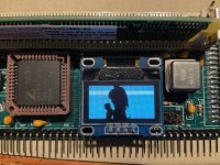
I tried removing the onboard Z80 and replacing it with external Z80. It will boot, but unable to run program in DRAM. I may not have wired WAIT or REFRESH correctly. However, I like to know the motivation for moving onboard Z80 to external Z80. Are you shooting for multiple Z80 sharing a common 32meg RAM?
I tried removing the onboard Z80 and replacing it with external Z80. It will boot, but unable to run program in DRAM. I may not have wired WAIT or REFRESH correctly. However, I like to know the motivation for moving onboard Z80 to external Z80. Are you shooting for multiple Z80 sharing a common 32meg RAM?