• Please review our updated Terms and Rules here

8 bit IDE (XTA) Replacement Project

Sure, in many of the traditional (2 cable) PC ESDI controllers, the behavior mirrors ATA, right down to the IDENTIFY command--something not supported in ST506-type controllers. It's not hard to see where the notion of IDE came from--certainly not from the ST506-interface drives.

Can't you connect an ST506-interface drive to an AT MFM controller card? To a PC, a 16 bit IDE drive looks like an AT MFM controller, with some additions added along the way. I was of the understanding that the IDENTIFY command did not come along until IDE drives were already in common use.

The 8 bit IDE (XTA) drives look to the PC like an original XT Xebec controller. I'm not sure there are any differences other than the meaning of the drive size bits. Sadly, no BIOS I have looked at hints at there being any kind of command for retrieving drive parameters.
 
The XTA interface boards came in. I assembled one to test. It seems to work with both the ST05X and WD BIOSes. At least with my ST351 A/X. I tested my WD93024-X drive with the WD BIOS and it just hung on boot. That drive stopped working in my TL/2 also so I think it is probably bad. Darn!

After ordering, I changed around some address lines so that it could at least be possible to program the flash ROM from the installed PC. Hence the bodge wires. I still need to do a bit more development to related to this.

I also need to make some changes for the bracket. I got the mounting holes wrong for the Keystone bracket I intended to use. Turns out that I can't find any off-the-shelf bracket that will fit without increasing the board dimensions past the magic 100x100mm size. Once the boards go past that dimension, the cost jumps sharply. Most, I need to take the board a little closer to the back of the PC. The one bracket I found with longer mounting tabs is a bit too high at the top of the board. I think this is about where folks add an unnecessary COM port as the cost of an assembled surface mount COM port + DB9 bracket from China costs about the same as the larger board and Keystone bracket.


Click image for larger version  Name:	IMG_20210927_194312470.jpg Views:	0 Size:	200.5 KB ID:	1226466 Click image for larger version  Name:	IMG_20210927_194324997.jpg Views:	0 Size:	182.0 KB ID:	1226465
 
jlcpcb usually. Their premium for exceeding 100x100 is relatively small.

Who doesn't do the 100x100 thing?

Ahh I also use JLCPCB but now I understand what the disconnect is. JLC only does the 100x100 limit on designs which qualify for their promotional prototype. If you exceed that size it no longer qualifies for the promotional price. However I get all my ISA cards in ENIG which doesn't qualify for the promotion regardless, and I see you got HASL
 
I also need to make some changes for the bracket. I got the mounting holes wrong for the Keystone bracket I intended to use. Turns out that I can't find any off-the-shelf bracket that will fit without increasing the board dimensions past the magic 100x100mm size.

Or you could get creative, rotate your Gerber files by a few degrees and use a slightly unconventional board outline.
Alternatively, just use the cheapest bracket you can find (without mounting tabs) and screw it to a pair of plastic blocks, which in turn you can screw to the board.
 
Ahh I also use JLCPCB but now I understand what the disconnect is. JLC only does the 100x100 limit on designs which qualify for their promotional prototype. If you exceed that size it no longer qualifies for the promotional price. However I get all my ISA cards in ENIG which doesn't qualify for the promotion regardless, and I see you got HASL

I do use ENIG on final boards. There is still a premium for those in small quantities for exceeding the magic size - about 1.5x. They actually give you a couple of extra mm before the price jumps, but I think I need just a little more than that. I think the hole will close, but the wall will be so thin.

Or you could get creative, rotate your Gerber files by a few degrees and use a slightly unconventional board outline.
Alternatively, just use the cheapest bracket you can find (without mounting tabs) and screw it to a pair of plastic blocks, which in turn you can screw to the board.

Rotating is an interesting idea. It would however need a substantial rotation to move the bottom hole back far enough. That would eat a lot of board real estate and turn a fairly easy to route board into a very challenging one. I suspect it would probably make assembly orders challenging too.

I'll bite the bullet and make it work with an off the shelf bracket. Just a little frustrating to be a few mm short. Keystone actually have a bracket that would work great in a catalog sheet but it has been discontinued. We are lucky though that ISA brackets are still available at all.
 
Attached is the ROM of the 1987 Zenith OEM Western Digital IDE-XT interface card I got on eBay. It is very early for any kind of IDE, but I was able to get it working with my WD93028-X drive. There is no formatting routine in ROM and it only works with Western Digital drives with sector translation enabled.

zds-idext-cr.jpg
 

Attachments

  • zdsidext.zip
    2 KB · Views: 3
Attached is the ROM of the 1987 Zenith OEM Western Digital IDE-XT interface card I got on eBay. It is very early for any kind of IDE, but I was able to get it working with my WD93028-X drive. There is no formatting routine in ROM and it only works with Western Digital drives with sector translation enabled.

Thanks! Great quality image of the front size of the board. Would it be possible to get a pic of the back side? I would like to check a couple of things about the circuit.
 
The rear of the card, including bodge:

Thanks again! I was able to confirm that like the Seagate card, the drive data lines are directly connected to the bus. That is good, since I implemented my board that way. The use of the LS244 and resistor bank for many of the signals is a little strange - seems to be buffering non-data lines. I can't see why that would be necessary unless some drive or some system was not behaving as it should. I suppose it is possible that is why my WD drive is not working with my card design. I will have to try to find an original WD card.

I disassembled the BIOS some. It is very small - just a bit over 2K. Copyright is Zenith, not WD. The low level format entry point jumps straight to the int 13 handler code (BIOS disk access functions). So that is not going to format anything :) At least some portions of the BIOS is not originally for IDE drives. The drive numbering assumes there are two drives on every interface. That is possible with the MFM controllers but not with XT-IDE. Second drives are on a second interface with XT-IDE.

The drive parameter table is different again from the other cards I looked at. 3 of the 4 drives in the table are the same ~20MB settings and one is for 32MB. I don't actually see any code which chooses anything other than the first entry (20MB). Oh, hey look, I can post in a table from Google Sheets. Comparisons below:
Drive TypeST05XWD-defaultWD-altOld Zenith BIOS
CylHeadsSize (bytes)CylHeadsSize (bytes)CylHeadsSize (bytes)CylHeadsSize (bytes)
03D4542,649,600264421,307,392267421,411,840264421,307,392
1267632,117,760267632,117,76030E320,419,58439D432,204,800
23D4542,649,6003D1542,519,04030E427,226,112264421,307,392
3267421,411,840267421,411,84030E213,613,056264421,307,392
ST351/AX when configured for ST05X per Tandy faxback instructions
ST325X
 
The rear of the card, including bodge:

The bodge is interesting. Looks like they got the reset backwards. That inverter's whole job seems to have been to invert the reset signal. After the bodge, reset is no longer inverted. However, they also added that R/C circuit (there is a bodge cap on the front side). I can't quite make sense of what that does - maybe the machine it was installed it had something odd with the reset.
 
I have been stuck in a bit of a loop with moving forward with the drive development - never feeling sure I had the optimal way to attach a microcontroller to the bus. I think I have found it now.

The Raspberry Pi Pico has a rather brilliant feature they call Programmable IO. It involves a very cleverly designed programmable state machine (really, a simple processor) with very flexible connections to the PIO pins, as well as FIFOs + IRQ control to connect to the main processors. The timing is very explicit and executes once instruction per clock cycle (125MHz apparently). On a 10 MHz ISA bus, that would be 50 instructions per ISA IO read/write cycle. Crazy. Crazy good.

It looks like a very interesting and challenging optimisation problem to program the PIO hardware. I think I am starting to get my head around it though, and it looks to me like it is extremely well suited to ISA devices. The only thing it I see that it looks poorly suited to is decoding large addresses - say port 388 out of a 10 bit port range. For the 2 bits of addressing needed for XTA and IBM 8 bit DBA drives, it like there are multiple good ways to handle that. By adding some additional address decoding logic I think it would be possible to implement a very capable PnP sound card with the PICO. It even has 2MB of built in flash memory.

The Pico also has a good number of pins, is very inexpensive and is likely to be around for a while. It has DMA to the PIO as well as the SPI (SD card). All the sample code I've seen indicates a clean and intuitive API. C/C++ support and Python for those who prefer that. The datasheet might be the best written I have ever read too.

I an pretty darn excited about the prospects.

The only down side is that the Pico is not 5v tolerant. That is going to drive me nuts as this drive replacement would otherwise have just been a Pico strapped to the bus and no other active components. It will be especially frustrating if singles of tri-state or open collector outputs are needed.

For anyone interested, I thought this was a good overview: https://hackspace.raspberrypi.org/articles/what-is-programmable-i-o-on-raspberry-pi-pico

Then this video: https://www.youtube.com/watch?v=yYnQYF_Xa8g

And then the PIO section of the RP2040 datasheet: https://datasheets.raspberrypi.org/rp2040/rp2040-datasheet.pdf
 
Two remarks:
- A 10 MHz ISA bus doe not mean the I/O is running at 10 MHz as well. The Turbo-XT boards I have insert at least one wait state when doing I/O. That enables them still to use the 5 MHz 8237 DMA IC and othe 5 MHz ICs. And if you are not sure about the speed, nothing stops you to use the IOCHRDY line to insert wait state by yourself.
- I'm not at home right now so I cannot check but what MPUs were the original drives using? Certainly not something that was equivalent to a Pi Pico. I think a Arduino would be more in line. And it would save your 5V problem.

Looking forward to your solution,

The original drives had additional hardware to support the micro. Seagate and WD both had custom chips that included the significant amount of glue logic needed. I am trying to minimize that extra logic as it adds to the problems of complexity/cost/dev effort/parts availability.

While the IBM drives can use IOCHRDY, the XTA drives to not have access to that signal. That would definitely change the conversation. I would use an AVR + GAL22V10 as the base.

There is some discussion on choice of micro earlier in this thread. The AVR's used in the original Arduino - I like them - but they are not nearly fast enough to listen to the ISA bus on their own. There is actually a SID replacement project I found that does do this for the C64 by rather massively overclocking the AVR. By my reading, it would need to be at least twice as fast again for the ISA bus. It looks like some ARM micros might be just about fast enough but the CPU timings gets less deterministic with higher performance. Most dump you into 3.3v land anyway.

There is one 5v all in one option - a Cypress micro part with a CPLD-like programmable logic section. The downsides are that it is a bit of an oddball part/toolchain, it is kind of pricey, and there is no practical option for easy hand soldering. I want to design something that is easy for someone to produce in small numbers.

I was originally going to go with AVR + CPLD, but the CPLD doesn't meet the high level drive current requirements for the ISA bus. I mean, I am pretty sure it would actually work in the target PC's which won't have 8 expansion cards in them. Seems prudent to stay in spec though. So it would still needs at least two additional 74 ICs and possibly one more.

The PIC32 looks promising - it has 4 built in 8 bit registers which greatly simplifies the needed glue logic. There are only a few 5v tolerant pins but that could be enough to save a level shifting chip. I think a pair of 74LVC245's would do the trick. The documentation/tool chain does not look amazing. Not sure it is a very future proof part to be basing things on. I was going to start working with it anyway until I discovered what the Pico can do.

The Pico, with its super-duper programmable IO, looks to be more than capable enough and also the easiest to experiment with. More fun too :) I think I will be able to easily prototype the whole solution on a breadboard. It will also need at least two 74LVC's to do the level shifting, and possibly one more. I have one already - hopefully I will get a chance to experiment with it soon.
 
The Tandy 1000RL can enable IOCHRDY, although leaving it off is the default and is listed as "PC compatible":

RL_ChipSelectsLarge.jpg
 
The Tandy 1000RL can enable IOCHRDY, although leaving it off is the default and is listed as "PC compatible":

RL_ChipSelectsLarge.jpg

That is interesting - I don't think it is necessarily related to hard drives though.

The ATA connector does have an IORDY signal so kind of odd that XTA does not. I just double checked and none of the standalone boards route that signal. There is no pin for IOCHRDY on the ST05X, WDXT-150 or the Zenith card.
 
I have been looking more at the programmable IO (PIO) on the Raspberry Pi Pico and this definitely looks like it is going to work. I have been giving a lot of thought on how best to write the PIO programs. I thought some others might find the topic interesting/useful. The Pico has a total of 8 PIO state machines and they are arranged like this:

Code:
        <--- FIFO <---
ARM CPU              PIO STATE MACHINE <---> OUTSIDE WORLD
        ---> FIFO --->

On both XTA and the IBM drives, one of the ports (and the DMA) performs contiguous reads/writes into a memory buffer. The FIFOs seem to be perfect for this. It is even possible to DMA from the Pico RAM to/from the FIFOs, making it possible to implement the entire 512 byte memory buffer without any demand on a Pico CPU.

The writes from the PC to other ports also look to be pretty easy. The drive implementation does not need to respond quickly to these except to latch a "busy" flag. I think any hardware device with a microcontroller in the mix must be the same (Sound Blaster DSP for example). So a second state machine can send the port address and data values into a FIFO and a Pico CPU can pull those out and process them at its leisure. The busy flag is a bit tricky - the state machines can't do much in the way of math on register values. However I think there is a way to use duplicate code paths, one that explicitly sets an output pin high, and another that sets the same output pin low.

The remaining two read ports are a little tricky. In all cases they hold status/flags values. The FIFOs are not super ideal for setting these - we want the value read by the PC to update immediately, not provide a history of the port values. The state machines do have effectively 3 registers to hold values (two temp registers and the last value off the FIFO) so in principle one state machine could service reads for 3 ports. However there is no way for a Pico CPU to get a value into the temp registers without pausing the state machine and then it would be unable to respond to reads from the PC. The easiest approach is probably to use an entire state machine per read port and have the state machine constantly pull the FIFO so the data stays up to date.

Someone I was talking to privately asked about performance of the state machines. There seems to be oodles of performance. By my reading of the ISA bus documentation I have looked at, the Pico would have two whole ISA bus cycles to perform its response to ~IOR or ~IOW going low. All PICO state machine instructions execute in one cycle. For ISA at 10MHz and a Pico at 125MHz, that would be 25 PIO state machine instructions. Even allowing a cycle for latency and some more for headroom, that seems like it will be at least twice what is needed. Sometimes the the instructions can even perform two operations using side channel functionally. For example, one instruction could set the direction on an externa bus transceiver and pull data from the FIFO. Even branches are always one cycle - none of the usual branch prediction, penalties if the branch is taken/not taken etc. It would be possible for example to use 4 branches to decode an entire 16 port range and only burn 4 cycles.

I did also figure out that the Pico could decode ISA IO addresses directly. One state machine can decode the address range and trigger other state machine(s) to handle the read/write. I think it might even be possible to implement an entire Sound Blaster Pro 2 on a Pico, sans DAC and 5v level shifting. Hard to be sure - there are 6 read registers on the SB Pro 2 and the complexity might burn a lot of instructions. That is a potentially tight limitation with PIO: only 32 instructions per 4 state machines.

Time to write some code. I do have a Pico up and running on a breadboard with a new hello-world project. Setting up the C++ SDK was more involved than Arduino but it and the documentation feel like professional tools to me. Better actually - all the source code is present too. It was still easier to set up than I have found other CMake projects to be. Great docs and a community build Windows setup tool very much helped. The Pico also seems well suited to field-upgrading firmware. It just needs to be connected to a computer via a micro-USB cable. It then shows up as a drive and the new firmware uf2 file is dragged over. I am sure it would also be possible to implement some kind of upgrade path using the vintage host PC but it is very nice to not have to implement something out of the gate.
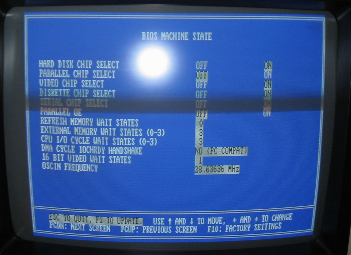
 
Last edited:
A bit of an update: I'm making baby steps forward. I was able to get some code running on the Raspberry Pi Pico programmable IO. It is pretty hardcode and delivers. I implemented a mock up of simplified ISA bus IO write timing. I will then use this to test my PIO code for handling ISA writes. The IO write takes 5 ISA bus clock cycles. When mimicking a 10MHz ISA bus, the Pico PIO program needs two instructions (each 1 pico-cycle) and then another 60 Pico-cycles of delays.
Code:
.program isaout
.side_set 1
    pull                side 1  ; Blocking pull from FIFO. FIFO is configured for 10 bit words (max 32).
    out pins, 10 [10]   side 1  ; Set 2 bit address and 8 bit data, then delay the rest of the ISA bus clock.
    nop [12]            side 0  ; Transition ~IOW low and hold for 3 ISA bus clocks.
    nop [11]            side 0
    nop [11]            side 0
    nop [12]            side 1  ; Transition ~IOW high and wait one more ISA bus clock.

The PIO state machine can be slowed down to minimize the amount of delay needed but this code is just for testing. It is bonkers how much performance there is to play with. I think I could even cram 8 bits of external shift register reads into the cycle. The Pico can run a little faster too if necessary - default is 125MHz and it is rated for 133Mhz. It does not surprise me so much that this is possible. Only that we went from there not really being much in the way of any good solutions, to this super flexible, high performance solution. A pic of it running:

IMG_20211017_134623202.jpg

The period is the expected 500ns. Here the PICO ARM CPU is doing continuous blocking writes into the FIFO with a plain-old-code loop and is keeping up just fine. I have been spoiled now - it will be hard to go back to an 8 bit micro for anything more complicated than a keyboard converter.

Before writing any more code, I decided to do a pass at a schematic so I could write the code in a semi-final way. I still need to add the SD card sockets but this will work for now.

8-bit-ide-35-first-pass.PNG

Not only did I need to add a 3rd IC for voltage level conversion, I also ran out of pins on the Pico and needed to add a shift register for configuration settings. It took some work to figure out but I did manage to use ICs that are readily available in through hole packages.

- Jayeson
 
Back
Top