• Please review our updated Terms and Rules here

Another Pet 2001N issue.

dabone

Veteran Member
Joined
Feb 26, 2009
Messages
1,287
Location
Chattanooga, TN - USA
I've got a 2001N board someone sent me to take a look at. It's a 320350 board, no crtc.
It was missing the Character Rom and a 6520.
I've burned a 28c16 for the Character Rom and put in a good 6520.
(EEPROM works fine in my 2001N board)

I found that the crystal was dead and swapped in one I grabbed off an old pc board (16mhz.)

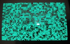
That brought the video back up. But it's just garbled, with a few characters kinda sparkling/changing.
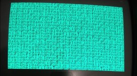
2001-n.jpg

I tested the 6502, 6522 and 6520 on my working 2001n. They all let my machine boot fine.

I also checked the roms (Basic 2) on my 2001n and the Kernal and one of the basic roms are dead.

I installed a Romulator, and went ahead and replaced the single wipe cpu socket with a dual wipe.

Reset circuit seems to be working correctly, held low for a short while, then high.

1Mhz Clock is present on the cpu.

I'm not getting any CAS on bank 0 or 1, so the Kernal isn't executing.

I've tried the following roms using the Romulator.
Pettester , Basic 2 Non-CRTC, Basic 4 Non-CRTC, Pet Low Ram Test, Pet RAM/ROM/VRAM Test.

When I enable the NOP generator on the Romulator, I'm getting pulsing on the cas lines. (Both ram banks)

Any suggestions on what to start checking next?

My available tools are Rigol 1054z scope, Logic Probe, lots of spare chips and sockets, multimeter, Another working pet.
 
I could be wrong, have to look it up, but I'm not sure if the pinout of the 28c16 is suited to replace the character ROM. The 2716 is. Pin 18 of the 28c16 is the /CE but the /EP (program enable) on the 2716 and there might be other differences, maybe look into that just in case. On pin 21; /WE on one and Vpp on the other. They might be compatible, I'm just not 100% sure, might not matter for a Read only situation rather than a programming one. The output enable is on the same pin, but it would pay to check the PET schematic. Also check that the 28c16 doesn't load down the /INIT line. Easy to check if the 28c16 behaves normally in your other PET.
 
First off, the /CAS lines have nothing to do with the Kernal ROM. No /CAS activity just indicates that either there is a fault in the /CAS logic or the CPU is not accessing RAM. Of course, this could be due to faulty ROM, but could also be due to a myriad of faulty devices on the data bus.

Can you enable my PETTESTER ROM in the ROMulator and map all of the RAM into the RAM on the ROMulator (if this is an option). Which ROMulator are you using?

What do you observe on the screen then?

I am expecting multiple faults from what I am observing on your initial screen.

The obvious first check would be CPU pin 7. Are there pulses on this pin (SYNC) indicating that the CPU is actually executing instructions.

It is interesting that the entire screen is in reverse video. This implies (but not guarantees) that the video RAM (data bit 7) is stuck high (F7) or the data latch (F9) or the D-flipflop (G9) is faulty in some way.

The screen display is also not as 'random' as I would have expected - thus indicating a similar issue with further video RAM data bits. There are two (2) video RAM devices - and one of these (I am guessing F7) could be faulty - thus accounting for the entire observed issue.

One thing you could try would be to remove the 6502 CPU (to stop any writes to video RAM on start-up); and scope F9 pins 13 and 12, and G9 pins 8, 9, 10, 11, 12 and 13. This would start to give us a clue as to what is going on.

It might also be prudent to scope all of the pins of F9 at the same time - as this may indicate further 'stuck' data bits.

Dave
 
Last edited:
I'm using the Romulator by bitfixer.

The romulator I'm using is mapping all ram / rom into the Romulator, I haven't enabled any pass thru ram configs yet.

I checked the 2114 video rams, and both are bad, I've replaced them with tested working ones, and now the screen appears like this.

This is with the Pettester rom enabled.


Selecting Basic 4 for the 2001N gives me a static garbage screen.

Screenshot 2023-04-27 060234.jpg

I do have activity on pin 7 of the 6502.
 
That is good. That looks like a pretty good 'random' screen now.

I wouldn't bother too much about the 'glitching' - this generally happens when running the PETTESTER's VDU screen test. It 'hammers' the video...

It does indicate that the video RAM is not being written to (however).

Can I ask you to have a look on pin 10 of the video RAM (devices F7 and F8) to see if the signal is either permanently HIGH or is going LOW also. HIGH is read and LOW is write.

If the signal is permanently HIGH, can you check device F6 pins 1, 5, 6, 7 and 15.

Pin 5 should be HIGH. Pin 15 should be LOW. Pin 1 should have a 1 MHz clock on it.

Pin 6 should go LOW on a CPU write access to the video RAM. If pin 6 doesn't go LOW - there are a couple of logic gates driving it that you can follow back to see where the signal is getting lost.

Dave
 
Ok, last one before I go to work...

Pin 10 has activity on both rams, and F6 1,5,and 15 are 1mhz, High, and Low as expected.
Pin 6 has activity.
 
Ok, just doing a visual inspection of the board, and it has some bodges that I think are factory?

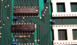
e6-e7.jpg

Trace cut in between E6 and E7.

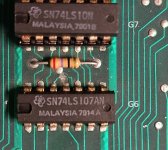
g6-g7.jpg

Trace cut between G6 and G7


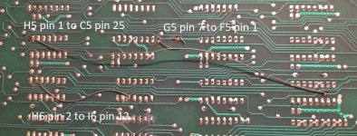
wires.jpg

Jumper wires on the back.

H5 Pin 1 to C5 Pin 25
G5 Pin 7 to F5 Pin 1
H6 Pin 2 to I6 pin 12

The board also has the old white single wipe sockets on the VIA and PIAs.

G7 is socketed, because I had it in my head that you needed ras and cas for dram refresh.. doh..
 
I have seen a factory modification to some of the PETs related to cutting tracks and jumpering. Not sure whether this is the same modification though.

I can see from the video that you posted (#4) that some display cells update correctly and then get overwritten - whereas others do not change at all. For example, I can see a lone of "@abcdefgh..." appearing (written to by the PETTESTER) and then they are overwritten.

This smacks of a faulty video address multiplexer (F3, F5 and/or F6). I would guess F3 or F5.

I am assuming that it is correctly passing the video counters through to the SAn lines, but not switching over to pass the BAn lines through to the SAn lines. For one half of the clock the buffered address lines are presented to the SAn lines and for the other half of the clock the video counters are presented to the SAn lines.

Dave
 
Last edited:
Thinking about it a bit more, it is also possible that the address buffers (B3 and/or C3) are duff.

To check these, enable the NOP generator from the ROMulator (assuming this is present) and scope the buffered address lines. BA0 should be 250 kHz and each higher address line should be half the previous frequency. So BA1 should be 125 kHz. and so forth.

Dave
 
How do you do that... :) You are the man!


C3.....

c3.jpg


I have to go babysit grandkids, so I don't have time to slap a new on in yet, but I do know that one was bad.
 
So the pet is up and running but with 16k ram. I've burned 2532 eproms for a Basic 4.0 set, and I'm using a 2816 for the edit rom/pet tester

Pet tester and Basic see 16K ram.


The jumpers (Shunts) on this board are strange, and don't match what I found on zimmers.

Currently SH1 is 001001 and SH2 is 1110000101
My other 2001n is like as found at zimmers SH1 001101, SH2 1111000101

Zimmers reference pic..


I jumpered the board I'm working on like mine and it made no difference.
The board I'm working on had 32k from the factory.


Now I'm hoping someone can explain something about the ram circuit that I just don't get.

This goes back to the CAS0 / CAS1 lines.

On page 6 of the schematics, G7 generates both cas lines, the only difference is the cas0 runs one input thru an inverter so the output is inverted.
They then go to r41 and r42, then onto the ram pin 15 per bank (Cas 0 low bank, Cas 1 high bank.)

Using a NOP generator, I get a nice inverted cas on both banks.

Why don't I see a inverse output on cas1 all the time? It's a steady high while the machine is running.
 
H4/Y4 being HIGH means that a CAS cycle is going to be produced on one of the banks of RAM devices.

The bank that is selected is based upon address line 14 (hence the inverter).

You will get a /CAS1 when both G7 pins 3 and 5 are HIGH (and the resulting output on pin 6 is LOW).

Now the 'rub'...

The 6502 CPU makes a lot of use of page 0 and 1 of the RAM (in the range $0000 to $01FF). As a result, you see a lot of /CAS0 activity. You only ever see /CAS1 activity when the program addresses RAM in the range $4000 to $7FFF.

PETTESTER has a 'sniff' at powers of two of RAM and (if a simple check fails) it calls it a day and only tests up to that point (-1).

The NOP generator is oblivious to any RAM that is fitted or not.

The way around this is to get the low bank of 16K fully working (with PETTESTER) and then swap over the /CAS lines to make the upper 16K bank map into the lower 16K - and then use PETTESTER...

I can explain this in more detail if you want to try it.

Dave
 
Since the DRAM control signals are constantly active, even if the computer is just sitting there not running a program after it boots up, I documented them in my PET in this condition with over 20 scope recordings including /CAS0 and /CAS1. They are on page 6 and 7 of this article:

www.worldphaco.com/uploads/DRAM%20MEMORY%20TEST%20SYSTEM%20FOR%20THE%20DYNAMIC%20PET%20COMPUTER.pdf

The easiest way to transpose the /CAS0 and /CAS1 control signals for the upper and lower bank is to lift one leg of each of the series 27 Ohm resistors and make the switch that way.

If you look at the overall upper and lower bank arrays you will see that all of their connections are common except the /CAS0 and /CAS1. So switching these swaps the two banks, which can be helpful for testing.

In my DRAM test system, outlined in the article linked above, it dynamically deactivates the lower 1k or 2k of DRAM, and switches in SRAM on a hardware adapter, to support BASIC and small programs, then the remainder of the DRAM can be tested. But if BASIC is working already, you could still use the ROM firmware in that article to test the DRAM memory. Four programs are placed in a 2532JL ROM and put in Socket UD3. One is a block move program, the other 3 are for memory diagnostics. The code is at the end of the article, it is not too long so that you can hand enter it in your programmer if you wanted. But the simpler thing to do is use the PETTESTER and simply swap the /CAS lines.
 
On this question:

"Why don't I see a inverse output on cas1 all the time? It's a steady high while the machine is running."

Looking at G7 the two gates which generate the /CAS0 and /CAS1 are wired as a data selector, to select the pulse from H4 pin 12 to /CAS0 or /CAS1.

(in 32k memory mode with that link set) and when the address line BA14 high /CAS1 is active and with BA14 low then /CAS0 is active.

So as Daver2 says, the pulses you see on /CAS0 and /CAS1 depend on the access of the upper and lower banks, and they also the relative timing of the pulses from pin 12 of H4. Therefore the pulses won't look complimentary.
 
I have no formal training, so sometimes I get a bit confused, but these explanations are great, I should have realized that it ba was controlling it, I just couldn't put it together in my head for some reason.
So thanks again, you guys are great.
 
Back
Top