• Please review our updated Terms and Rules here

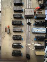
Anyone recognize this Apple ][ clone motherboard?

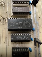
Sorry, I do not have an EPROM reader for a working system. Here are some additional pictures of some of the chips that are hard to read in the other pictures. This board comes from a person with a ton of vintage computer hardware and he wasn't sure about where this one was from. It was with a few other Apple ][ motherboards and an Apple ][ clone made by NorTel (not at all licensed I don't believe). He may have just had it with them because it had spare parts.20221030_165209982_iOS.jpg20221030_165344560_iOS.jpg20221030_165435427_iOS.jpg20221030_170035159_iOS.jpg
 
Whelp, looks like my surety in that black chip being ROM was sorely misplaced, it appears to be a 6850 ACIA.

Initially eyeballing this it looks like the data and addressing lines for the SRAM are pulled over from the same set connected to the EPROMs, so… maybe it *is* there as a DMA accessible buffer for the serial chip? (They’re using the SRAM instead of DMA to the DRAM because of timing constraints?) This seems like major overkill for an RS-232-speed terminal application, so… I’m genuinely baffled now.
 
… that all said, an alternative theory I could be convinced by is the SRAM isn’t the character buffer memory, it could be for storing a user defined character set? There’s a certain attraction to that idea now that it’s popped into my head. If that is what it’s for its proximity to a character ROM still makes sense, and it also sets up the CRTC to be the source of DRAM refresh, sharing access with the 6502 on opposite sides of the clock.
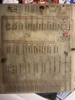
Ya that could of be true, When I originally looked at the board it was in low resolution view. This board could have a buffer to store a user defend character set. The boards owner did post a couple more pictures of the PCB, especially the bottom view (to help release it secrets). Some of the unreadable IC part number are now visible so we can find out what they are.
 
Last edited:
… that all said, an alternative theory I could be convinced by is the SRAM isn’t the character buffer memory, it could be for storing a user defined character set? There’s a certain attraction to that idea now that it’s popped into my head. If that is what it’s for its proximity to a character ROM still makes sense, and it also sets up the CRTC to be the source of DRAM refresh, sharing access with the 6502 on opposite sides of the clock.
Whelp, looks like my surety in that black chip being ROM was sorely misplaced, it appears to be a 6850 ACIA.

Initially eyeballing this it looks like the data and addressing lines for the SRAM are pulled over from the same set connected to the EPROMs, so… maybe it *is* there as a DMA accessible buffer for the serial chip? (They’re using the SRAM instead of DMA to the DRAM because of timing constraints?) This seems like major overkill for an RS-232-speed terminal application, so… I’m genuinely baffled now.
I did hint about that in a pervious message especially if they were using a MC6852 SSDA or a mC6854 ADLC communication chip. The MC6850 will support data communications up to 1M Bits per second with the use of an external buffer on a system with a slow microprocessor clock rate. see https://pdf1.alldatasheet.com/datasheet-pdf/view/4161/MOTOROLA/MC6850.html
If the board bottom circuits traces where in a different pattern, I would have a better ideal about it.
 
Whelp, looks like my surety in that black chip being ROM was sorely misplaced, it appears to be a 6850 ACIA.

Initially eyeballing this it looks like the data and addressing lines for the SRAM are pulled over from the same set connected to the EPROMs, so… maybe it *is* there as a DMA accessible buffer for the serial chip? (They’re using the SRAM instead of DMA to the DRAM because of timing constraints?) This seems like major overkill for an RS-232-speed terminal application, so… I’m genuinely baffled now.
Yes, that can be a DMA based serial port buffer or a memory mapped Serial port buffer used for hi speed communication, since the MC6850 can do up to 1M bits per second. See my other entry for a like to a better data sheet in HTML format.
 
Refresh could be as brute force as a having an IRQ run 128 NOPs out of RAM every millisecond.
There are other ways to do refresh with the 6502 and MC6800 microprocessors, on some controllers they use a 555 timer to trigger an NMI or INT when itis time to do a memory refresh cycle. Normally they have a memory overlay that is switch in when the refresh routine has to be run. (In short)
 
I did hint about that in a pervious message especially if they were using a MC6852 SSDA or a mC6854 ADLC communication chip. The MC6850 will support data communications up to 1M Bits per second with the use of an external buffer on a system with a slow microprocessor clock rate. see https://pdf1.alldatasheet.com/datasheet-pdf/view/4161/MOTOROLA/MC6850.html

Maybe I'm missing something, but where do you get the part about an "external buffer" being something that comes naturally to this chip? I did some light reading on the 6850 and the conclusion I've come to is it's pretty unlikely the SRAM is specifically a DMA buffer for it. Here's an article that goes into pretty good depth about the use of the 6850, and between that and the datasheet it looks like trying to do DMA to an external buffer it would require quite a lot of glue. (Long and short of it, you'd need an external DMA controller to do address generation, and on top of that you'd need to design an autonomous state machine that can either listen for generated interrupts from the chip and/or constantly poll the status registers of the chip to know when a new character is available. And for this DMA controller we'd also need another set of address multiplexers for the RAM so both this DMA controller and the CPU could alternate ownership of it, which there are no sign of. Most of the ICs in the next row are simple 7400 and 7404-level glue logic.)

And, FWIW, the datasheet does say you can clock the serial side of the "B" version of the chip at up to 1Mhz, and with a 2Mhz 6800 or 6502 you'd probably have just enough CPU oomph available to grab bytes off it and shove them into RAM with tight polling loop, but because of how bus cycles work on those chips it actually wouldn't really matter if the target memory was SRAM or DRAM, memory wait states aren't really a thing for those CPUs. (Everything is synchronous for those chips. Usually, anyway.) Also, FWIW, for the chip to operate at that 1Mhz serial speed (IE, run in "1x mode") it requires an external data separator circuit. This board already seems kind of "sparse". The 6850 makes way more sense as a low-speed serial engine, IE, RS-232-speed serial. I mean, yeah, anything's possible, but...

Of course, what would really help a ton is if we could find where the baud rate generator is on this thing(*); there's a still a lot of chips that are unreadable, and, honestly, the pictures are fragmentary and unaligned enough it's making my head hurt to try to follow traces from one side to the other. (And a fair number of trace/via junctions are hidden by components.) I'm back to leaning towards the SRAM being the character memory for the video output as the most likely theory and they just happened to put the SRAM and the serial chip adjacent to each other (and near the ROMs) because, well, that makes sense because all of those devices need the un-multiplexed version of address bus. But... who the heck knows. Since I don't have the thing in my hand to poke at with a continuity tester I think I'm inclined to yield.

(* Up near the DIP switches is a counter, multivibrator, and other parts that *might* be baud rate generation? This thing is a mess.)
 
Last edited:
Maybe I'm missing something, but where do you get the part about an "external buffer" being something that comes naturally to this chip? I did some light reading on the 6850 and the conclusion I've come to is it's pretty unlikely the SRAM is specifically a DMA buffer for it. Here's an article that goes into pretty good depth about the use of the 6850, and between that and the datasheet it looks like trying to do DMA to an external buffer it would require quite a lot of glue. (Long and short of it, you'd need an external DMA controller to do address generation, and on top of that you'd need to design an autonomous state machine that can either listen for generated interrupts from the chip and/or constantly poll the status registers of the chip to know when a new character is available. And for this DMA controller we'd also need another set of address multiplexers for the RAM so both this DMA controller and the CPU could alternate ownership of it, which there are no sign of. Most of the ICs in the next row are simple 7400 and 7404-level glue logic.)

And, FWIW, the datasheet does say you can clock the serial side of the "B" version of the chip at up to 1Mhz, and with a 2Mhz 6800 or 6502 you'd probably have just enough CPU oomph available to grab bytes off it and shove them into RAM with tight polling loop, but because of how bus cycles work on those chips it actually wouldn't really matter if the target memory was SRAM or DRAM, memory wait states aren't really a thing for those CPUs. (Everything is synchronous for those chips. Usually, anyway.) Also, FWIW, for the chip to operate at that 1Mhz serial speed (IE, run in "1x mode") it requires an external data separator circuit. This board already seems kind of "sparse". The 6850 makes way more sense as a low-speed serial engine, IE, RS-232-speed serial. I mean, yeah, anything's possible, but...

Of course, what would really help a ton is if we could find where the baud rate generator is on this thing(*); there's a still a lot of chips that are unreadable, and, honestly, the pictures are fragmentary and unaligned enough it's making my head hurt to try to follow traces from one side to the other. (And a fair number of trace/via junctions are hidden by components.) I'm back to leaning towards the SRAM being the character memory for the video output as the most likely theory and they just happened to put the SRAM and the serial chip adjacent to each other (and near the ROMs) because, well, that makes sense because all of those devices need the un-multiplexed version of address bus. But... who the heck knows. Since I don't have the thing in my hand to poke at with a continuity tester I think I'm inclined to yield.

(* Up near the DIP switches is a counter, multivibrator, and other parts that *might* be baud rate generation? This thing is a mess.)
Kind of missed it, but anyways
"external buffer" on this board is likely not used, but I have not mapped out the unused pins on to ACIA chip co confirmed that.
It does come fairly easy if you add a few external components. You can do DMA transfers old school without a DMA Controller with just some 74lsXXX logics and some type of counter chip/shift register. (The shift register generates the address buses address for the buffer memory).
As for the constantly poll the status registers of the serial chip to know when a new character is available, why waste the microprocessor resources on that, even at 2MHZ if you have to send packet data as well as the Serial data bits. As for the article at http://alanclements.org/serialio.html it is prey general,
does not cover MILITARY uses of the 6850 or more complex uses of the 6850 ACIA chip where buffering is required (used).
The design an autonomous state machine can be done in some more simple logic chips. Most 6502 have a RDY and Clock input and output signals that's all that's needed, (plus the Sync signal pin). There are other ways to share a bus without the use of multiplexers. (But I leave it out - someone else could comment on that).
..
As far as this thing is a mess, I did hint about the PCB Board layout in a previous message.
Yes, even with the board's owners updated pictures, there's a still a lot of chips that are unreadable, and, honestly, the pictures are fragmentary and unaligned (likely used a buds/somebody cell phone to take some rushed pictures). There's still no picture of the boards bottom side with the full IDC connector shown. I did not follow the traces back to their locations, Nore did I redraw the PCB from the pictures. There is a fair amount traces hidden by components and several jumpers that somebody should trace out.
..
 
Last edited:
Hopefully the boards owner will upload some more pictures (photos) so the baud rate generator can be found.
Ya the counter, multivibrator, and other parts could be an old school be baud rate generation? Or they could be recovering the serial ports clock rate from the serial data received. Could also be using the video clock for this purpose as well (if used as an alarm monitor controller).
..
The SRAM being the character memory for the video output as the most likely theory, but it could also be for a Custom Character generator/Graphic Image buffer as well. (No SDCA, HDLC Controller)
The board would still have to be mapped out to see if it supports gray scale or wither its B&W only.
..
Hopefully some other reader in this forum is in the board owner location and can arrange to dump its firmware contance to this forum. Doing a test with a continuity tester would release some more data about it.
..
If this board is from a remote alarm monitor system them the ACIA in its location is likely for remote monitoring by a serial device. This would provide an interpterion of what's being digitized. The receive channel side of the ACIA would be for remote control and the status control of it.
Some what related thought - Anybody who delt with the cost of sending video through the telephones companies lines back in the 1980's knows the cost advantage of using serial communications format over it (, wither it was a leased line or not).
..
As far as serial port buffering even on the IBM PCXT with any 3270, Twinaximal, or early network boards, they all had a buffer. The 16550 series UARTs incorporated a 16-byte FIFO buffer inside the chip.
..
Hopefully the board owner soon sends us some updates. (Pictures and whatever else they can).
 
As for the constantly poll the status registers of the serial chip to know when a new character is available, why waste the microprocessor resources on that, even at 2MHZ if you have to send packet data as well as the Serial data bits. As for the article at http://alanclements.org/serialio.html it is prey general,
does not cover MILITARY uses of the 6850 or more complex uses of the 6850 ACIA chip where buffering is required (used).

Out of curiosity, do you happen to *have* any examples of a 6850 being used in a DMA application? A broad suggestion that some secret military application used it that way is great and all, but all the design examples I could find using it are far, far simpler. We're talking "Apple II Super Serial Card", not high-powered network packet engines.

And the point about polling it: you don't know if a "fresh" data byte is available unless you read the flag, nor do you know when it's clear to send, which with this chip is a distinct bus operation you need to interleave with read/writes, which if you're not doing it with the CPU you'll need to build into your state machine. There were contemporary UARTs like the TR1602 that would be far easier to make discrete-logic DMA state machines for because they directly expose pins that say if the send/receive buffers are clear or full. There are way better choices than the 6850 for an unattended high-speed data streamer.

It does come fairly easy if you add a few external components. You can do DMA transfers old school without a DMA Controller with just some 74lsXXX logics and some type of counter chip/shift register. (The shift register generates the address buses address for the buffer memory).

Yes, you can build an address generator out of discrete parts, but where is it? Remember, to make use of the amount of SRAM on this board you're going to need 11 bits; there are 12 bit ripple counters, but they wouldn't be a great general-purpose choice for a DMA controller since they can only count from 0 to X, there's no preload. A more sophisticated counter would be more parts...

here are other ways to share a bus without the use of multiplexers. (But I leave it out - someone else could comment on that).

Not on the original 6502. Full stop. It has no built-in mechanism to tri-state its address bus, unlike the 6800 its bus mostly apes nor like the 8080/Z80 family. Even if you halt it for DMA operation with the RDY line you still need external circuitry to switch it off. This was a major driver for Commodore to cook its oddball variants of the 6502 like the 6510 which have built-in tristate. (The modern WDC65C02 also has internal tristate, I've actually used it on a breadboard computer to share RAM between the CPU and video memory.)

(Edit: The "SALLY" variant of the 6502 in the Atari 8-bit family also had internal tristate.)

As far as serial port buffering even on the IBM PCXT with any 3270, Twinaximal, or early network boards, they all had a buffer. The 16550 series UARTs incorporated a 16-byte FIFO buffer inside the chip.

But the plain old IBM PC/XT serial port had the 8250, with no built in FIFO, and the AT used the 16450, likewise with no FIFO(*). For modem-speed serial communication (given the vintage of this board we're talking 300 to maybe 2400 baud) a plain dumb CPU-driven serial implementation seems far more likely then there being some elaborate DMA state machine being hidden in this small handful of circuitry. Even if this was the heart of a locally-driven serial terminal it probably only ran at 9600-19200 baud, which a 6502 should be able to handle reasonably with PIO as long as it's not trying to multitask anything.

(* By the 1990's PC serial ports had mostly switched to the 16550, but I have a 1995-vintage 486 laptop that still has a fifo-less 16450 embedded in its chipset.)
 
Last edited:
I'll try to take some better, more uniform pictures of the motherboard so all the components can be read and pieced together.
 
The standard MC6850 from 1978 will support up to 500K bps - Confirmed from my 1978 "The Complete Motorola Microprocessor Data Library" book.
Other data I have confirmed from the 3Rd party Advance Applications notes for the MC6850 ACIA.
..
Tristate or no tristate on the 6502 microprocessors, yes, some 3RD parity and newer versions had it built it.
But with the clock signals on the 6502 microprocessors that do not support it
Out of curiosity, do you happen to *have* any examples of a 6850 being used in a DMA application? A broad suggestion that some secret military application used it that way is great and all, but all the design examples I could find using it are far, far simpler. We're talking "Apple II Super Serial Card", not high-powered network packet engines.

And the point about polling it: you don't know if a "fresh" data byte is available unless you read the flag, nor do you know when it's clear to send, which with this chip is a distinct bus operation you need to interleave with read/writes, which if you're not doing it with the CPU you'll need to build into your state machine. There were contemporary UARTs like the TR1602 that would be far easier to make discrete-logic DMA state machines for because they directly expose pins that say if the send/receive buffers are clear or full. There are way better choices than the 6850 for an unattended high-speed data streamer.


Yes, you can build an address generator out of discrete parts, but where is it? Remember, to make use of the amount of SRAM on this board you're going to need 11 bits; there are 12 bit ripple counters, but they wouldn't be a great general-purpose choice for a DMA controller since they can only count from 0 to X, there's no preload. A more sophisticated counter would be more parts...


Not on the original 6502. Full stop. It has no built-in mechanism to tri-state its address bus, unlike the 6800 its bus mostly apes nor like the 8080/Z80 family. Even if you halt it for DMA operation with the RDY line you still need external circuitry to switch it off. This was a major driver for Commodore to cook its oddball variants of the 6502 like the 6510 which have built-in tristate. (The modern WDC65C02 also has internal tristate, I've actually used it on a breadboard computer to share RAM between the CPU and video memory.)

(Edit: The "SALLY" variant of the 6502 in the Atari 8-bit family also had internal tristate.)


But the plain old IBM PC/XT serial port had the 8250, with no built in FIFO, and the AT used the 16450, likewise with no FIFO(*). For modem-speed serial communication (given the vintage of this board we're talking 300 to maybe 2400 baud) a plain dumb CPU-driven serial implementation seems far more likely then there being some elaborate DMA state machine being hidden in this small handful of circuitry. Even if this was the heart of a locally-driven serial terminal it probably only ran at 9600-19200 baud, which a 6502 should be able to handle reasonably with PIO as long as it's not trying to multitask anything.

(* By the 1990's PC serial ports had mostly switched to the 16550, but I have a 1995-vintage 486 laptop that still has a fifo-less 16450 embedded in its chipset.)

, you can simulate it by using external logic and decoding the full clock cycles.
 
Out of curiosity, do you happen to *have* any examples of a 6850 being used in a DMA application? A broad suggestion that some secret military application used it that way is great and all, but all the design examples I could find using it are far, far simpler. We're talking "Apple II Super Serial Card", not high-powered network packet engines.

And the point about polling it: you don't know if a "fresh" data byte is available unless you read the flag, nor do you know when it's clear to send, which with this chip is a distinct bus operation you need to interleave with read/writes, which if you're not doing it with the CPU you'll need to build into your state machine. There were contemporary UARTs like the TR1602 that would be far easier to make discrete-logic DMA state machines for because they directly expose pins that say if the send/receive buffers are clear or full. There are way better choices than the 6850 for an unattended high-speed data streamer.


Yes, you can build an address generator out of discrete parts, but where is it? Remember, to make use of the amount of SRAM on this board you're going to need 11 bits; there are 12 bit ripple counters, but they wouldn't be a great general-purpose choice for a DMA controller since they can only count from 0 to X, there's no preload. A more sophisticated counter would be more parts...


Not on the original 6502. Full stop. It has no built-in mechanism to tri-state its address bus, unlike the 6800 its bus mostly apes nor like the 8080/Z80 family. Even if you halt it for DMA operation with the RDY line you still need external circuitry to switch it off. This was a major driver for Commodore to cook its oddball variants of the 6502 like the 6510 which have built-in tristate. (The modern WDC65C02 also has internal tristate, I've actually used it on a breadboard computer to share RAM between the CPU and video memory.)

(Edit: The "SALLY" variant of the 6502 in the Atari 8-bit family also had internal tristate.)


But the plain old IBM PC/XT serial port had the 8250, with no built in FIFO, and the AT used the 16450, likewise with no FIFO(*). For modem-speed serial communication (given the vintage of this board we're talking 300 to maybe 2400 baud) a plain dumb CPU-driven serial implementation seems far more likely then there being some elaborate DMA state machine being hidden in this small handful of circuitry. Even if this was the heart of a locally-driven serial terminal it probably only ran at 9600-19200 baud, which a 6502 should be able to handle reasonably with PIO as long as it's not trying to multitask anything.

(* By the 1990's PC serial ports had mostly switched to the 16550, but I have a 1995-vintage 486 laptop that still has a fifo-less 16450 embedded in its chipset.)
Yes the plain old IBM PC/XT serial port had the 8250, with no built in FIFO, but where are noteing about farrly low speed serial communication.
The FIFO was added to the 16550 to help stop character lost at higher data transfer rates, that would happen on the 16450 version. (At the same data rate).
 
As far as polling the MC6850 that's fine for lower speed data communications, but the MC6850 has a RTS (output) and CTS (input) signal pins for the serial ports' signals, so use them instead of polling. It is easy to build logic to detect when a "fresh" data byte is available without polling.
..
A short not on the MC6850 ACIA chip (for other readers how are not too familiar with it.) Just some basic crap about it.
The Mc6850 ACIA does have signals pins for: /CTS and /RTS, /DCD, Rx data, TC data, Rx clk input, Tx clk input.
Enable input can be used as a Data Strobe and Clock latch strobe. On some systems the Address bus is also active when this signal is active.
/IRO output can be combined with CTS and RTS signals to emulate wither the Transmit channel side or Receive Channel side has a Int.
..
On some systems the Mc6850 CS signal is inverter to RS232C leaves and is combined with /RTS to form the /DTR signal.
The RI (Ring indicated) is tied to the DCD signal and sometimes also to the CTS signal.
As far as RI, DTR and DSR these signals could always be routed to an unused PIA port for enhanced serial port status.
..
3 CS signal lines plus 1 RS signal pin is used to select between the Data register and the Status control registers. The RD//WR signal controls the Bus direction.
the maximum data rate early versions support is 500K Bits per second (without overclocking caching)
the number of data bits is 8 bit and the rest of the information someone could always look up (if they wish to).

The standard MC6850 from 1978 will support up to 500K bps - Confirmed from my 1978 "The Complete Motorola Microprocessor Data Library" book.
Other data I have confirmed from the 3Rd party Advance Applications notes for the MC6850 ACIA.
..
Tristate or no tristate on the 6502 microprocessors, yes, some 3RD parity and newer versions had it built it.
But with the clock signals on the 6502 microprocessors that do not support it


, you can simulate it by using external logic and decoding the full clock cycles.
The 6502 Microprocessor
As far as being MotorolaMC6800 bus compatible, with the full decoding of all the 6502 Clock cycle signals (, yes input and outputs ones) you can fully simulate
all of the MC6800 bus signals. They can be simulated in the 6502 clock signals, but you must externally decode them.
Bus Available (BA), Data Bus Enable (DBE) also known as 02 clk or E signal are encoded on the microprocessors clock pins.
External HALT(Stop) and it's acknowledged signal is usually done by external logic circuity.
..
Technically the 6502 has Three state control status emulation/simulation encoded on its multiphase clock cycle signals pins, but most boards don't interment it and on most simple hardware it is not used anyways. Real Three state control is available on some advances 3Rd party clones, so some extra external logic is not needed.
..
Yes, the original 6502 has no built-in mechanism to tri-state its address bus, but you can emulate it with a small circuit built with a flip-flop.
You can temporary pause (or wipe the microprocessors memory) the 6502 microprocessors by external manipulation of its clock input signal.
..
DMA or IDMA emulation with the 6502 microprocessors
You can Nore Gate the 6502 microprocessor o2Clk out pin 39 with the 0O clock signal on Pin 37 to generate a S01 Clock signal is used for compatible VPMA Access and NOVPMA access signals.

..
You can pull the microprocessor 01 clock high just after a 02 clock cycle to suspend the microprocessor for 4 system 01 clock cycles before destroying data within the microprocessor. This hidden TSC time then can be used in a short DMA application. With a custom burst control circuit, you can transfer 8 bytes in this time slot if the memory can support it. (Limited by the bandwidth of memory logic). This is mostly undocumented 6502 data.
The Sync signal line with the use of the o1 clock signal and the RDY signal can be used to single step the microprocessors instructions.
The IRQ signal is sampled during a 02 clock operation, if the microprocessor is set for interrupts it would start on the next 01 Clock cycle (on some variants its timing is somewhat different).
..
Note: Clk=Clock
..
The 6502 02 clock signal is the same as E signal on the MC6821 PIA
At least Commodore (MOS Technologies) with the 6510 built in the tristate logics removing some external logic that helps reduce the microprocessor customer products cost.
 
Last edited:
DMA operation on the 6502 microprocessors with the use of the RDY line, yes you still need external circuitry to switch it off. (Wow another simple like flip-flop circuit for that). To handle BUSREQ and BUSACK signals on the 6502 we used another flip-flop circuit for that.
 
Out of curiosity, do you happen to *have* any examples of a 6850 being used in a DMA application? A broad suggestion that some secret military application used it that way is great and all, but all the design examples I could find using it are far, far simpler. We're talking "Apple II Super Serial Card", not high-powered network packet engines.

And the point about polling it: you don't know if a "fresh" data byte is available unless you read the flag, nor do you know when it's clear to send, which with this chip is a distinct bus operation you need to interleave with read/writes, which if you're not doing it with the CPU you'll need to build into your state machine. There were contemporary UARTs like the TR1602 that would be far easier to make discrete-logic DMA state machines for because they directly expose pins that say if the send/receive buffers are clear or full. There are way better choices than the 6850 for an unattended high-speed data streamer.


Yes, you can build an address generator out of discrete parts, but where is it? Remember, to make use of the amount of SRAM on this board you're going to need 11 bits; there are 12 bit ripple counters, but they wouldn't be a great general-purpose choice for a DMA controller since they can only count from 0 to X, there's no preload. A more sophisticated counter would be more parts...


Not on the original 6502. Full stop. It has no built-in mechanism to tri-state its address bus, unlike the 6800 its bus mostly apes nor like the 8080/Z80 family. Even if you halt it for DMA operation with the RDY line you still need external circuitry to switch it off. This was a major driver for Commodore to cook its oddball variants of the 6502 like the 6510 which have built-in tristate. (The modern WDC65C02 also has internal tristate, I've actually used it on a breadboard computer to share RAM between the CPU and video memory.)

(Edit: The "SALLY" variant of the 6502 in the Atari 8-bit family also had internal tristate.)


But the plain old IBM PC/XT serial port had the 8250, with no built in FIFO, and the AT used the 16450, likewise with no FIFO(*). For modem-speed serial communication (given the vintage of this board we're talking 300 to maybe 2400 baud) a plain dumb CPU-driven serial implementation seems far more likely then there being some elaborate DMA state machine being hidden in this small handful of circuitry. Even if this was the heart of a locally-driven serial terminal it probably only ran at 9600-19200 baud, which a 6502 should be able to handle reasonably with PIO as long as it's not trying to multitask anything.

(* By the 1990's PC serial ports had mostly switched to the 16550, but I have a 1995-vintage 486 laptop that still has a fifo-less 16450 embedded in its chipset.)
Yes, I have documentation on the MC6850 ACIA being used with buffers and IDMA logic in storage. (Mostly on a nondisclosure bases).
Mostly for: Multiplexed data Terminal Packet Multiplexers, several old Burroughs ASYNC Poll-select Terminal equipment clones, Various military and industrial controllers that use a serial packet protocol. This chip has been used in some external storage devices/controllers where the MC6850 is doing the serial/parallel conversions at a high data rate. (Mostly in none IBM data format).
..
I have seen hardware where an ACIA was used instead of a MC6840 PTM clip with 1 channel active, it has also been used as a video shift register with a MC3480 DRAM RFH Ctrl doing the Hor and Ver line driving. I have also seen this chip driving speakers instead of a more expensive sound chip.
..
Yes, there are better choices than the 6850 for an unattended high-speed data streamer (, but they were not always used (, mostly $$$$)).
..
There are other ways then to use 12-bit ripple counters without preload capability, at one time their where 12-bit shift register available (with and without the xxxload pin.
..
The MC6850 has a RTS (output) and CTS (input) signal pins for the serial ports signals, that can be used for the state machine (logics) with the Int signal you can detect wither the transmit or receive channel has the interrupt. So why write code and waste some of the microprocessor time on this task so you can use higher data transfer rates than by polling the ACIA chip.
..

For other reader who are not too knowledgeable with the MC6850 serial data format.
Normally the MC6850 can only send and receive a 10-bit character frame, but some enhanced clones can send a 12-bit character frame (one of the CS lines is used differently). One Start bit, 8-data bits, one parity bit, and 2 stop bits. 8- and 9-bit data with the fixed user of the parity bit.
 
Last edited:
Out of curiosity, do you happen to *have* any examples of a 6850 being used in a DMA application? A broad suggestion that some secret military application used it that way is great and all, but all the design examples I could find using it are far, far simpler. We're talking "Apple II Super Serial Card", not high-powered network packet engines.

And the point about polling it: you don't know if a "fresh" data byte is available unless you read the flag, nor do you know when it's clear to send, which with this chip is a distinct bus operation you need to interleave with read/writes, which if you're not doing it with the CPU you'll need to build into your state machine. There were contemporary UARTs like the TR1602 that would be far easier to make discrete-logic DMA state machines for because they directly expose pins that say if the send/receive buffers are clear or full. There are way better choices than the 6850 for an unattended high-speed data streamer.


Yes, you can build an address generator out of discrete parts, but where is it? Remember, to make use of the amount of SRAM on this board you're going to need 11 bits; there are 12 bit ripple counters, but they wouldn't be a great general-purpose choice for a DMA controller since they can only count from 0 to X, there's no preload. A more sophisticated counter would be more parts...


Not on the original 6502. Full stop. It has no built-in mechanism to tri-state its address bus, unlike the 6800 its bus mostly apes nor like the 8080/Z80 family. Even if you halt it for DMA operation with the RDY line you still need external circuitry to switch it off. This was a major driver for Commodore to cook its oddball variants of the 6502 like the 6510 which have built-in tristate. (The modern WDC65C02 also has internal tristate, I've actually used it on a breadboard computer to share RAM between the CPU and video memory.)

(Edit: The "SALLY" variant of the 6502 in the Atari 8-bit family also had internal tristate.)


But the plain old IBM PC/XT serial port had the 8250, with no built in FIFO, and the AT used the 16450, likewise with no FIFO(*). For modem-speed serial communication (given the vintage of this board we're talking 300 to maybe 2400 baud) a plain dumb CPU-driven serial implementation seems far more likely then there being some elaborate DMA state machine being hidden in this small handful of circuitry. Even if this was the heart of a locally-driven serial terminal it probably only ran at 9600-19200 baud, which a 6502 should be able to handle reasonably with PIO as long as it's not trying to multitask anything.

(* By the 1990's PC serial ports had mostly switched to the 16550, but I have a 1995-vintage 486 laptop that still has a fifo-less 16450 embedded in its chipset.)
As far as 11-bits that really mostly for a one way buffering the D2114 has only 10 address lines A0 to A9 so there are some things you could do with the extra bit.
Rip counters ok, but at one time there was 11 and 12-bit shift register available (with a count up and down capacity). Or you could build one out of a bunch of flip-flop circuits.
 
you can simulate it by using external logic and decoding the full clock cycles.

But that was my point: that "external logic" is either multiplexers or tri-state buffers (which add up to the same thing); everyone and their dog making home computers with the 6502 made use of the "I only use the bus on the Phi0/2 low phase" behavior of the 6502 to interleave video and CPU access to memory without explicit wait states, but doing that relied on an external multiplexer to let video or whatever device drive the bus. It's not "free" on the 6502.

Yes, the original 6502 has no built-in mechanism to tri-state its address bus, but you can emulate it with a small circuit built with a flip-flop. (...)

Okay, citation/clarification needed at this point. What are you talking about? You say this and then you talk about ways to pause the clock without using the RDY signal... which, sure, that's a technique some 6502 based computers used when they needed to do something that required more time than PHI1 for an operation (generically I've seen this called "clock-stretching"), but it has *nothing* to do with tri-stating the bus other than it's something you're likely to do *while* you're tri-stating the bus with those external buffers you've installed for that.

As for all the blather about the specific differences in the control/clock signals between the 6800 and the 6502, that is *way* out there in the weeds and irrelevant to this whole discussion. I mentioned the 6800 in passing only because the 6800 happens to have built-in Tri-State. The pin the 6502 calls "RDY" is called "HALT" on the 6800, and when HALT-ed the 6800 tri-states the bus. Here is the only MOS datasheet which documents the 6501, which was the "socket compatible" version of the 6502 which used the same external clocking components as the 6800, and it documents this difference in behavior on page 8.

And regardless, those differences that do exist between the 6800 and 6502 are mostly irrelevant to the family of support chips that Motorola designed for the 6800 family and MOS ruthlessly cloned. Both families of chips use the method of watching the clock phase to know when they should be active; on Motorola datasheets it's E, on MOS datasheets it's PHI. That's all *they* care about.


The standard MC6850 from 1978 will support up to 500K bps - Confirmed from my 1978 "The Complete Motorola Microprocessor Data Library" book.
Other data I have confirmed from the 3Rd party Advance Applications notes for the MC6850 ACIA.

Yes, I read the datasheet. Did you notice the caveat that when operating in 1x mode it requires an external data separator, all the features to do bit synchronization/framing are disabled if you run it that fast? It basically turns into a shift register with parity checking.

And again, quoting the datasheet is not an example of a real-world application of this device in a high-speed streaming (w/DMA) mode.
Yes the plain old IBM PC/XT serial port had the 8250, with no built in FIFO, but where are noteing about farrly low speed serial communication.
The FIFO was added to the 16550 to help stop character lost at higher data transfer rates, that would happen on the 16450 version. (At the same data rate).

Yes. My question is why you're so over-the-top convinced that this device needs faster than that and is built accordingly. Because it sure doesn't look that way.

Anyway. I spent a little time squinting at the circuit board (which I think I'm done doing; if someone wants to send it to me I'd be willing to spend a few hours probing it, but probably on the condition I'm allowed to break it down for spare parts afterwards unless it does turn out to be interesting somehow.) Here's what I came away with; I'm not 100% sure about any of it but it's the best I think I can get out of the pictures here and, frankly, not being able to actually touch the thing with a continuity tester:
  • The data lines for the SRAMs and EPROMs are directly connected and also appear to directly terminate on the CPU.
  • Address lines from the CPU also go directly to the EPROMs. So it does not appear to be possible to drive the EPROM address lines from addresses generated by the CRTC.
  • The above means that either this thing only spits out bitmapped graphics or it uses RAM-defined character sets.
  • The PROM next to the SRAMs appears to be the main chip select/decoder.
  • Trying to trace the RAM address lines makes me cry. Most of the traces are under chips or dive through VIAs constantly. But...
  • The two socketed chips at the far end of the row of EPROMs are probably the tri-state for the address lines so the CRTC can drive the RAM address lines. The markings are only visible on one of them, but if both are 74LS244Ns then that works.
  • I suspect the 74LS273N and the unreadable chip to the right of the 6850 are a video data latch and the pixel output shift register respectively.
  • There is *ZERO* evidence of any kind of DMA state machine for that 6850. It does have its IRQ line connected.
  • I don't think CTS, DCD, or RTS are even connected to the 6850. There are no traces visible on either side to pins 5, 23, or 24. This is not something that suggests high speed communication. At all.
  • Here's a real kicker. I don't think Rx Data is connected to the 6850 either. The transmit line is connected, but there is nothing on pin 2.
I'm actually starting to wonder if it's possible at least that this could be part of a video game or something. In which case:

I have also seen this chip driving speakers instead of a more expensive sound chip.

This 6850 shoved in there as a crude DAC looks like a real possibility with the way it's wired.
 
Last edited:
Thanks for clarifying,
Sorry about any confusion, my data sheets the clock signals are labeled differently. (Aka their named differently 00Clk, 01Clk and etc.,).
..
As far as you question, why I was so over-the-top convinced that this device needs faster than that and is built. In a pervious posting I had stated that I had see
similar PCB layout on synchronous based data terminal and related equipment, and in another posting I did note that my first looks at the PCB were in low resolution.
..
With the updated pictures, yes it sure doesn't look that way. It is centrally not a Sync communication device. I wasn't really that over the top about it, but I gust it is see that way, owell them. The use of the MC6850 is somewhat misconceiving in this PCB board design, they could have done a cheaper solution if it was for slow speed serial data communication.
..
Thanks for positing you analyst of his board, as I never did trace any of the logic traces, (no real free time for me to do that). I just went by component size and location and then their part numbers.
..
With the unconnected pins on the MC6850, I wonder if this board from the 1980 has hidden conductor traces in the middle layer or not?
Thats kind of a waste for the MC6850 when the use on a shift register would have been cheaper, but as a crude DAC maybe it was cheaper than a real DAC.
But wither that would be cheaper than an old school DAC made out of resistors, unknown
..
Hopefully some one reads its firmware and them post it to this form in the future. I would like to re Ass it, then read its Ass code. Ya the probing of it would be interesting.
..
Yes, it is likely part on something, could be part on a video game system, or something else, but it's unlikely a data terminal as is unlikely a data logger.
 
Back
Top