• Please review our updated Terms and Rules here

Build your own PDP 8I, Part 3..

Hi All;

Dave, Thanks for the Responses..

""Can I ask you to double-check the work you have done today please. ""

Yes.. I have a feeling that, on the first four bits, it had two wires to each MBxx pin, and so It was easy to find the one going to the 7489's, which I switched..
But, on the Last eight bits, there was only One wire, and I switched it, But the other wire may have been on the 7489's instead of the 74175's and it got switched as well, unknowingly..
So I will check these connections as well..

"" Your CLL CML will "set" the LINK register. ""
I know this, This was my Intent..

"" The DCA will clear AC after it has finished. ""
This I didn't Realize.. My Bad..

"" A bit more about the TAD instruction (I think I can see where things are going wrong).

The TAD instruction (during the EXECUTE phase) uses the value in MB (from the FETCH phase) to add to the AC and store the result in AC during CP0. You can see this on schematic LD15 at the logic leading up to G15 input pin 3. The AND and TAD instructions gate AC(L) during CP0.

On schematic LD15, MB(L) is gated at F5. So the FETCH state machine should be cycling F0, F1, F2, F3 (this is the same as before) but then F4 (not A4) followed by F5 and then terminated by A6.

Interestingly (with your single step of my C:=A+B program) I am seeing the COMPLEMENT of the memory location stored in MB!

The output from MB should still drive the front panel lamps and go to the MUX that feeds one input of the ALU. MB should ***ONLY*** be inverted for feeding the data inputs to the 7489 RAMs (and NOT for anything else). ""

I will Check them all..

I figured Out the Problem with the LED Display, They were wired to the 7489's, and Not to the 74175's..
So, when I switched the 7489's to /MB the Display showed the Wrong Value, because it was tied to /MB and Not MB..
The MUX on bit '0' is correct along with the 74133 bit '0'..
The 74133 has been checked out, it is wired correctly..
The First four of the MUXes have been checked and are wired Correctly..
The First four of the Led Drivers were wired to the 7489's and are being Fixed..
The Middle four of the Led Drivers are wired to the 7489's and are being fixed..
The Middle four of the Muxes are wired Wrong, and have been fixed and checked..
The Last four of the Led Drivers are wired to the 7489's and are being fixed..
The Last four of the Muxes are wired Wrong, and have been fixed and checked..
With What All I am finding Wired Wrong, I am surprised that it Ran at all..

THANK YOU Marty
 
Last edited:
Hi All;

Now to Re-do Dave's Test..

""
0000 7300 ; CLA CLL - Clear accumulator and link registers
0001 1006 ; TAD 6 - Load the number in memory location 6 (the number A) into the accumulator.
0002 1007 ; TAD 7 - Add the number in memory location 7 (the number B) to the accumulator.
0003 3010 ; DCA 8 - Deposit the answer (C) into memory location 8.
0004 7402 ; HLT - Stop so we can see the answer.
0005 5000 ; JMP 0 - Repeat on the next CONT.
0006 0001 ; The number A.
0007 0002 ; The number B.
0010 0000 ; The answer C = A + B. ""

It Doesn't hit halt..
But,
On schematic LD15, MB(L) is gated at F5. So the FETCH state machine should be cycling F0, F1, F2, F3 (this is the same as before) but then F4 (not A4) followed by F5 and then terminated by A6.

No, it does F0, F1, F2, F3, A4, CP0, etc..

I am going to call it quits for the night..

In the middle of the night (now) I figured out that our signal to pin 4 of the 74150, may not be changing state, when we are doing a DCA Instruction, (or a JMS or a JMP) as I think it should.. So that it should go to F4 and Not A4..
I will need to monitor that next time I have time to do so..

Tomorrow, I will be busy either all day or Most of it..
But, I think we have made some good Progress today..

"" You shouldn't need to insert HLTs to debug any program - just hit SINGLE STEP and CONT for each instruction to execute next... ""

I think I see the Answer after looking thru Your simple program..

"" Now we can run a very simple program successfully, fill all of memory with a NOP instruction (7000).

Set PC=0000
Set AC=1234

CONT

The machine should run forever...

STOP

Set the "SINGLE STEP" switch.

Set PC=0000

CONT.

A single FETCH/EXECUTE cycle should be processed and then the machine should stop with PC=0001.

CONT.

A single FETCH/EXECUTE cycle should be processed and then the machine should stop with PC=0002.

etc. etc. etc. ""

YES, Now that I have wired in the Single Step Switch..


"" Set the "SINGLE STEP" switch. ""
I have a PushButton, and You are referring to a Switch..
I have an Extra switch above the PushButtons, that was used in the Old machine, Only I could not remember what for..
So, I can wire it in parallel with the PushButton, and have a momentary Single Step, or a Set Single Step Switch..
And then Hopefully it will work, Just as You have Indicated.. And I won't need to Keep on Inserting Halts, all over the place..

I have wired it in, and it Works !!!!
I didn't know about Doing that before, that is on How to rightly use the Single Step Switch.. I like it !!!!

0000 7300 ; CLA CLL - Clear accumulator and link registers
0001 1006 ; TAD 6 - Load the number in memory location 6 (the number A) into the accumulator.
0002 1007 ; TAD 7 - Add the number in memory location 7 (the number B) to the accumulator.
0003 3010 ; DCA 8 - Deposit the answer (C) into memory location 8.
0004 7402 ; HLT - Stop so we can see the answer.
0005 5000 ; JMP 0 - Repeat on the next CONT.
0006 0002 ; The number A.
0007 0004 ; The number B.
0010 0000 ; The answer C = A + B.

Single Stepping it with a Slow Clock and it works, I changed the numbers,
But, Location '0010, does show '0006 !!!!!!!!!!!!

When Running a Faster Clock, it produces Garbage.. I will later need to determine what Top Clock speed it will work correctly..

THANK YOU Marty
 
Last edited:
"With What All I am finding Wired Wrong, I am surprised that it Ran at all.." - I aren't Marty. I have deliberately kept away from the memory until now - so that the memory and the MA/MB registers were kept out of the equation. Then we added MA/M to IR into the equation - and found a few problems (as expected) and then started to add new instructions into the mix (and found another problem with the inverted MB wiring yet again) - so don't despair - we have squashed a lot of bugs and I am expecting to squash a few more before the job is done yet...

I didn't explain the FETCH cycle differences too well did I? OPR/IOT and JMP/JMS/DCA instructions with direct addresses should go F0 ... F3, A4. But AND/TAD instructions (with direct addresses) should go F0 ... F3, F4, F5, A6. The extra two cycles (F4 and F5) are to get the instruction operand from memory into the MB register for the EXECUTION phase of the instruction.

There is no (logical) difference between the STOP button and the SINGLE INSTRUCTION switch - they both cause the next FETCH cycle to be halted after execution of the current instruction.

In the case of the STOP button - you need to keep it pressed until CP7 - whereupon the PDP machine will STOP (as it says on the tin). When you take your finger off the STOP button - it returns to the 'non STOP' state - but you have to press CONT to continue of course.

SINGLE INSTRUCTION on the other hand is a true on/off switch (i.e. when you press CONT it will always cause cessation of the next FETCH cycle after the current FETCH/EXECUTE cycle).

The STOP pushbutton should be wired to G9 pin 2 (on schematic LD9) and the SINGLE INSTRUCTION switch to G9 pin 13 on the same schematic.

I think we need to 'regroup' now (since you have done a little bit of circuit surgery). I would have though a wire-wrapped card should have been ok to 1MHz or so. It would be worth having a little play to see at what frequency things work OK - but in reality I think there is another bug lurking somewhere for us to find...

I will have a think over the next couple of days of some more tests in a bit more of a logical order than throwing a number of instructions and addressing modes we have not tested together before.

I have a few days of intense work now; so can I suggest you do a few more tests of your own with the OPR/JMP instructions to see if things work as you expect after the circuit surgery?

Dave
 
Last edited:
Hi All;

Dave, Thanks for the Message and the clarification..

"" we have squashed a lot of bugs and I am expecting to squash a few more before the job is done yet... ""

A Bug a Day keeps the doctor quit Busy..

"" I think we need to 'regroup' now (since you have done a little bit of circuit surgery). I would have though a wire-wrapped card should have been ok to 1MHz or so. It would be worth having a little play to see at what frequency things work OK - but in reality I think there is another bug lurking somewhere for us to find... ""
You may be right..
I had it working at a higher Frequency with the Bit Counting..
So, maybe something like (an IC) in this circuit path is not right, slow, or something like that..
I think trying some different instructions and seeing which ones will run at the faster rate and which one won't.. Might point out the problem..

I will have a think over the next couple of days of some more tests in a bit more of a logical order than throwing a number of instructions and addressing modes we have not tested together before.
OK..
I have a few days of intense work now; so can I suggest you do a few more tests of your own with the OPR/JMP instructions to see if things work as you expect after the circuit surgery? ""
OK..

""
"With What All I am finding Wired Wrong, I am surprised that it Ran at all.." - I aren't Marty. I have deliberately kept away from the memory until now - so that the memory and the MA/MB registers were kept out of the equation. Then we added MA/M to IR into the equation - and found a few problems (as expected) and then started to add new instructions into the mix (and found another problem with the inverted MB wiring yet again) - so don't despair - we have squashed a lot of bugs and I am expecting to squash a few more before the job is done yet... ""

Dave, here is something a little closer to Your Home..
https://www.youtube.com/watch?v=FAquli648l0

THANK YOU Marty
 
Last edited:
Marty, interesting reading! I wanted to mention that I purchased a copy of 'The Art of Digital Design'. The book you and some of the guys were talking about in some earlier post. I must admit that I think that I may get the hang of this 'mixing logic'. If I had this kind of stuff in school I don't remember. But, I'm sure it will help now. Thanks, Mike
 
Hi All;

Mike, Glad to hear that this might be of some Help..
I am wondering if You saw the other references to my other Dec pdp's, for Your reading pleasure, and so You don't make the same mistakes as I did..

THANK YOU Marty
 
Hi All;

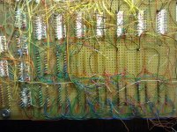
I have started to wire for the larger memory..
There are some Ic's that were on the Old system, that I don't have room for on my main Board..
And I had to Steal some 18 pin sockets from this Board..
So it will require some extensive rewiring, to make it work again..
Dave for Now, just assume that I still have the 7489's, until I tell You different..


001.jpg

As You can see, I have aways to go..

THANK YOU Marty
 
Last edited:
Mike_Z,

Welcome to our little corner of VCF!

Glad to hear that you read our thread - I am also an avid reader of your PDP-8 resurrection. Very nice barn/workshop find! (Although I am somewhat green with envy...)

Nice to see you are doing an absolutely superb job of refurbishment...

I was about to chip-in on the negative/positive logic debate in your thread - but have been a bit busy of late with work. Needless to say that the only reason that 'positive +5V' logic has 'won out' to some extent is a bit like the VHS vs Betamax debate. The +5V 74-series TTL logic family and the 8-bit micro revolution has popularised this 'type' of logic system. But (in the dim and distant days) there were a plethora of logic systems in use. For example, why +5V and 0V to mean logic '1' and '0'? It is only 'convention'. Why not 0V to mean logic '1' and +5V to mean logic '0'? Or -5V to represent logic '1' and 0V to represent logic '0'.

I am modifying a DMX512 laser unit and (after obtaining the schematics from the manufacturer) found that the microprocessor (an 8051 look-alike which is normally powered from +5V) is actually connected to a -5V power supply rail! 0V being effectively -5V and +5V being 0V. When I examined the schematic more closely - it was clear why they did it (a beautiful means of saving money on the product) - but it didn't half confuse me to start with.

Just to really confuse you (!) take a look at the 74181 that we use for our ALU http://www.ic.unicamp.br/~cortes/mc613/material_complementar/74HC_HCT181_Philips.pdf. If you scroll down to page 5 of the data sheet you will see that you can use this self-same device in an active low or active high logic context. The same is true of any logic family - so for example, a 7408 positive logic AND gate could be used as a negative logic OR gate!!!!!! (see http://www.dsm.fordham.edu/~moniot/Classes/CompOrganization/boolean-outline/node11.html)

As both Marty and myself have found out - you need to write 0-11 on a piece of paper and put it on the wall in front of your working area to remind you that 0 is the most significant bit and is on the left and 11 is the least significant bit and is on the right. You will keep forgetting - until it becomes second nature and then you have to think about modern microprocessors again...

Dave
 
Hi Marty,

I see you have started to upgrade your PDP-8...

Next block of tests now I have finished this hectic week.

JMP INSTRUCTION

Deposit the following program into memory:

0000 5017 JMP 17
0001 5016 JMP 16
0002 5015 JMP 15
0003 5014 JMP 14
0004 5013 JMP 13
0005 5012 JMP 12
0006 5011 JMP 11
0007 5010 JMP 10
0010 5000 JMP 0
0011 5007 JMP 7
0012 5006 JMP 6
0013 5005 JMP 5
0014 5004 JMP 4
0015 5003 JMP 3
0016 5002 JMP 2
0017 5001 JMP 1

Set the PDP-8 for SINGLE INSTRUCTION execution and step through the program one instruction at a time (starting from PC=0000 and AC=1234). Make sure your single stepping follows the mnemonics (for example, we start out by jumping to location 17 which then jumps to location 1 which then jumps to location 16 and so forth until it gets to location 10 whereupon the sequence begins again by jumping back to location 0).

If single-stepping seems OK, switch off SINGLE INSTRUCTION mode and let it run at full speed. AC should never change from 1234 during the run.

Dave
 
Last edited:
TAD INSTRUCTION - DIRECT operands.

Deposit the following program into memory:

0000 1017 TAD 17
0001 1016 TAD 16
0002 1015 TAD 15
0003 1014 TAD 14
0004 1013 TAD 13
0005 1012 TAD 12
0006 1011 TAD 11
0007 1010 TAD 10
0010 7777
0011 0002
0012 0140
0013 0220
0014 0410
0015 1004
0016 2002
0017 4001

STOP CLEAR (make sure L=0 and AC=0000).

Set PC=0000.

SINGLE STEP instruction stream from PC=0000.

AC should start out with 0000. Then '1' bits should start to accumulate from the left and right as each instruction is executed.

AC=0000 L=0 Before executing any instructions.
AC=4001 L=0 After executing the instruction at location 0000.
AC=6003 L=0 After executing the instruction at location 0001.
AC=7007 L=0 After executing the instruction at location 0002.
AC=7417 L=0 After executing the instruction at location 0003.
AC=7637 L=0 After executing the instruction at location 0004.
AC=7777 L=0 After executing the instruction at location 0005.
AC=0001 L=1 After executing the instruction at location 0006. Note the value in the LINK register!
AC=0000 L=0 After executing the instruction at location 0007. Note the value in the LINK register!

You can't step any further after instruction 0007 as you run into a list of constants.

Dave
 
Last edited:
I have a test program for AND with direct operands when you are ready - and then we can branch into JMS instructions with both direct and indirect operands next.

Dave
 
Hi All;

Dave, Thank You for the next set of Tests..

I am Jumping all over with Excitement over this test..

"" JMP INSTRUCTION

Deposit the following program into memory:

0000 5017 JMP 17
0001 5016 JMP 16
0002 5015 JMP 15
0003 5014 JMP 14
0004 5013 JMP 13
0005 5012 JMP 12
0006 5011 JMP 11
0007 5010 JMP 10
0010 5000 JMP 0
0011 5007 JMP 7
0012 5006 JMP 6
0013 5005 JMP 5
0014 5004 JMP 4
0015 5003 JMP 3
0016 5002 JMP 2
0017 5001 JMP 1

Set the PDP-8 for SINGLE INSTRUCTION execution and step through the program one instruction at a time (starting from PC=0000 and AC=1234). Make sure your single stepping follows the mnemonics (for example, we start out by jumping to location 17 which then jumps to location 1 which then jumps to location 16 and so forth until it gets to location 10 whereupon the sequence begins again by jumping back to location 0).

If single-stepping seems OK, switch off SINGLE INSTRUCTION mode and let it run at full speed. AC should never change from 1234 during the run. ""

OK !!!!!

"" TAD INSTRUCTION - DIRECT operands.

Deposit the following program into memory:

0000 1017 TAD 17
0001 1016 TAD 16
0002 1015 TAD 15
0003 1014 TAD 14
0004 1013 TAD 13
0005 1012 TAD 12
0006 1011 TAD 11
0007 1010 TAD 10
0010 7777
0011 0002
0012 0140
0013 0220
0014 0410
0015 1004
0016 2002
0017 4001

STOP CLEAR (make sure L=0 and AC=0000).

Set PC=0000.

SINGLE STEP instruction stream from PC=0000.

AC should start out with 0000. Then '1' bits should start to accumulate from the left and right as each instruction is executed.

AC=0000 L=0 Before executing any instructions.
AC=4001 L=0 After executing the instruction at location 0000.
AC=6003 L=0 After executing the instruction at location 0001.
AC=7007 L=0 After executing the instruction at location 0002.
AC=7417 L=0 After executing the instruction at location 0003.
AC=7637 L=0 After executing the instruction at location 0004.
AC=7777 L=0 After executing the instruction at location 0005.
AC=0001 L=1 After executing the instruction at location 0006. Note the value in the LINK register!
AC=0000 L=0 After executing the instruction at location 0007. Note the value in the LINK register!

You can't step any further after instruction 0007 as you run into a list of constants. ""

OK !!!!!!!!!!!!!!!

"" I have a test program for AND with direct operands when you are ready - and then we can branch into JMS instructions with both direct and indirect operands next. ""

Go ahead and post them, This way, once You go and do other things, I have the afternoon to try these out. and then I can let You know If there is a problem..
You'LL see the results tomorrow morning, soon enough..

I am going to Run Both of these programs first, then, see how fast and long each one will run..

THANK YOU Marty
 
Last edited:
MARTY STOP...

I have made a booboo and made a couple of significant edits to my last posts - pick them up first and don't use the ones you have just reposted.

DAve
 
Hi All;

Dave, Thank You for the Correction, I have re-copied Your Programs..

Good thing, I was working on the Memory Board, see picture, that I just inserted.. (above)

THANK YOU Marty
 
AND INSTRUCTION - DIRECT operands.

The intention of this program is to set all the bits of AC to '1' and shift a '0' bit in from the left-hand and right-hand side with the execution of each AND instruction with a constant held in memory.

STOP CLEAR.

Deposit the following program into memory:

0000 7240 CLA CMA
0001 0017 AND 17
0002 0016 AND 16
0003 0015 AND 15
0004 0014 AND 14
0005 0013 AND 13
0006 0012 AND 12
0007 0011 AND 11
0010 5000 JMP 0
0011 7777
0012 7637
0013 7557
0014 7367
0015 6773
0016 5775
0017 3776

Set PC=000 and AC=1234 before running. Set the SINGLE INSTRUCTION switch to 'on' and single step through the instructions one at a time with CONT.

After executing instruction 0000, AC should equal 7777.
After executing instruction 0001, AC should equal 3776.
After executing instruction 0002, AC should equal 1774.
After executing instruction 0003, AC should equal 0770.
After executing instruction 0004, AC should equal 0360.
After executing instruction 0005, AC should equal 0140.
After executing instruction 0006, AC should equal 0000.
After executing instruction 0007, AC should equal 0000.

After executing instruction 00010, AC should still equal 0000 but the PC should have been set back to 0000.

Continuing to single-step the program should result in the same thing as described above.

If this is the case, switch off SINGLE INSTRUCTION mode and run it at full speed.

Dave
 
Last edited:
AND instruction - auto indexed operand plus ISZ direct operand.

OK Marty - this will test your wire-wrapping!

STOP CLEAR.

Deposit the following program into memory:

0000 7240 CLA CMA
0001 0410 AND I 10
0002 2007 ISZ 7
0003 5001 JMP 1
0004 7402 HLT
0005 5004 JMP 4
0006 7402 HLT
0007 7771 Number of times to iterate around the ISZ loop.
0010 0011 Pointer to the 'AND' mask to use for the AC.
0011 3776 Consecutive mask words for the AC...
0012 5775 "
0013 6773 "
0014 7367 "
0015 7557 "
0016 7637 "
0017 7777 "

Set PC=000 and AC=1234 before running. Set the SINGLE INSTRUCTION switch to 'on' and single step through the instructions one at a time with CONT.

The instruction at address 0001 (AND I 10) should logically 'AND' the accumulator with the word that it finds indexed by memory address 0010. As memory address 0010 is one of the 'auto incrementing' locations - the value should be incremented by 0001 every time it is used. It initially points to the first mask word to use.

The instruction at address 0002 (ISZ 7) should increment memory address 0007 (used as a counter) and skip the 'JMP 1' instruction if the counter wraps over from 7777 to 0000 (i.e. the end of the count loop). If not, the instruction at address 0003 is not skipped (it is executed) and a loop is performed back to the instruction at address 0001.

The registers should proceed as follows (where PC is the program counter, AC is the accumulator, [7] is the contents of memory location 0007 and [10] is the contents of memory location 0010):

(Note that there is a 'JMP 1' instruction at memory address 0003 that I have not included here as it doesn't modify register AC or the memory locations of interest - but it does occur after each and every ISZ 7 instruction that requires the loop to continue (i.e. to seethe PC back to 0001 for the next AND I 10 instruction).

PC=0001 AC=7777 [7]=7771 [10]=0011 (Before AND I 10 instruction).

PC=0002 AC=3776 [7]=7771 [10]=0012 (After AND I 10 instruction but before ISZ 7 instruction).
PC=0001 AC=3776 [7]=7772 [10]=0012 (After ISZ 7 instruction but before AND I 10 instruction).

PC=0002 AC=1774 [7]=7772 [10]=0013 (After AND I 10 instruction but before ISZ 7 instruction).
PC=0001 AC=1774 [7]=7773 [10]=0013 (After ISZ 7 instruction but before AND I 10 instruction).

PC=0002 AC=0770 [7]=7773 [10]=0014 (After AND I 10 instruction but before ISZ 7 instruction).
PC=0001 AC=0770 [7]=7774 [10]=0014 (After ISZ 7 instruction but before AND I 10 instruction).

PC=0002 AC=0360 [7]=7774 [10]=0015 (After AND I 10 instruction but before ISZ 7 instruction).
PC=0001 AC=0360 [7]=7775 [10]=0015 (After ISZ 7 instruction but before AND I 10 instruction).

PC=0002 AC=0140 [7]=7775 [10]=0016 (After AND I 10 instruction but before ISZ 7 instruction).
PC=0001 AC=0140 [7]=7776 [10]=0016 (After ISZ 7 instruction but before AND I 10 instruction).

PC=0002 AC=0000 [7]=7776 [10]=0017 (After AND I 10 instruction but before ISZ 7 instruction).
PC=0001 AC=0000 [7]=7777 [10]=0017 (After ISZ 7 instruction but before AND I 10 instruction).

PC=0002 AC=0000 [7]=7777 [10]=0020 (After AND I 10 instruction but before ISZ 7 instruction).
PC=0004 AC=0000 [7]=0000 [10]=0020 (After ISZ 7 instruction. The PC will have moved on to the HLT instruction at address 0004).

The PDP-8 should halt.

To re-run the program (e.g. at full speed) you will have to set memory locations 0007 back to 7771 and 0010 back to 0011 (these two memory locations are used by the ISZ and AND I instructions respectively and are updated as a result).

This is my 'first pass' through this test. I may have got something wrong somewhere - so I will re-check it after lunch. If the register values are a bit confusing I will try and describe my program a bit better for you. What may be obvious to me when I am writing it may not be obvious to anyone else trying to read what I have written (what I call "write once read never" code)...

Dave
 
Last edited:
Hi All;

DAVE, I am truely amazed at what You have put out. It doesn't matter whether it actually works or not, that I am amazed..

I will try these Tomorrow morning..

"" AND INSTRUCTION - DIRECT operands.

The intention of this program is to set all the bits of AC to '1' and shift a '0' bit in from the left-hand and right-hand side with the execution of each AND instruction with a constant held in memory.

STOP CLEAR.

Deposit the following program into memory:

0000 7240 CLA CMA
0001 0017 AND 17
0002 0016 AND 16
0003 0015 AND 15
0004 0014 AND 14
0005 0013 AND 13
0006 0012 AND 12
0007 0011 AND 11
0010 5000 JMP 0
0011 7777
0012 7637
0013 7557
0014 7367
0015 6773
0016 5775
0017 3776

Set PC=000 and AC=1234 before running. Set the SINGLE INSTRUCTION switch to 'on' and single step through the instructions one at a time with CONT.

After executing instruction 0000, AC should equal 7777.
After executing instruction 0001, AC should equal 3776.
After executing instruction 0002, AC should equal 1774.
After executing instruction 0003, AC should equal 0770.
After executing instruction 0004, AC should equal 0360.
After executing instruction 0005, AC should equal 0140.
After executing instruction 0006, AC should equal 0000.
After executing instruction 0007, AC should equal 0000.

After executing instruction 00010, AC should still equal 0000 but the PC should have been set back to 0000.

Continuing to single-step the program should result in the same thing as described above.

If this is the case, switch off SINGLE INSTRUCTION mode and run it at full speed. ""

YES !!!!, It Works !!!!!!!!!!!!!! And RUNS ...............

"" AND instruction - auto indexed operand plus ISZ direct operand.

OK Marty - this will test your wire-wrapping!

STOP CLEAR.

Deposit the following program into memory:

0000 7240 CLA CMA
0001 0410 AND I 10
0002 2007 ISZ 7
0003 5001 JMP 1
0004 7402 HLT
0005 5004 JMP 4
0006 7402 HLT
0007 7771 Number of times to iterate around the ISZ loop.
0010 0011 Pointer to the 'AND' mask to use for the AC.
0011 3776 Consecutive mask words for the AC...
0012 5775 "
0013 6773 "
0014 7367 "
0015 7557 "
0016 7637 "
0017 7777 "

Set PC=000 and AC=1234 before running. Set the SINGLE INSTRUCTION switch to 'on' and single step through the instructions one at a time with CONT.

The instruction at address 0001 (AND I 10) should logically 'AND' the accumulator with the word that it finds indexed by memory address 0010. As memory address 0010 is one of the 'auto incrementing' locations - the value should be incremented by 0001 every time it is used. It initially points to the first mask word to use.

The instruction at address 0002 (ISZ 7) should increment memory address 0007 (used as a counter) and skip the 'JMP 1' instruction if the counter wraps over from 7777 to 0000 (i.e. the end of the count loop). If not, the instruction at address 0003 is not skipped (it is executed) and a loop is performed back to the instruction at address 0001.

The registers should proceed as follows (where AC is the accumulator, [7] is the contents of memory location 0007 and [10] is the contents of memory location 0010):

AC=7777 [7]=7771 [10]=0011 (Before AND I 10 instruction).

AC=3776 [7]=7771 [10]=0012 (After AND I 10 instruction but before ISZ 7 instruction).
AC=3776 [7]=7772 [10]=0012 (After ISZ 7 instruction but before AND I 10 instruction).

AC=1774 [7]=7772 [10]=0013 (After AND I 10 instruction but before ISZ 7 instruction).
AC=1774 [7]=7773 [10]=0013 (After ISZ 7 instruction but before AND I 10 instruction).

AC=0770 [7]=7773 [10]=0014 (After AND I 10 instruction but before ISZ 7 instruction).
AC=0770 [7]=7774 [10]=0014 (After ISZ 7 instruction but before AND I 10 instruction).

AC=0360 [7]=7774 [10]=0015 (After AND I 10 instruction but before ISZ 7 instruction).
AC=0360 [7]=7775 [10]=0015 (After ISZ 7 instruction but before AND I 10 instruction).

AC=0140 [7]=7775 [10]=0016 (After AND I 10 instruction but before ISZ 7 instruction).
AC=0140 [7]=7776 [10]=0016 (After ISZ 7 instruction but before AND I 10 instruction).

AC=0000 [7]=7776 [10]=0017 (After AND I 10 instruction but before ISZ 7 instruction).
AC=0000 [7]=7777 [10]=0017 (After ISZ 7 instruction but before AND I 10 instruction).

AC=0000 [7]=7777 [10]=0020 (After AND I 10 instruction but before ISZ 7 instruction).
AC=0000 [7]=0000 [10]=0020 (PC will have moved on to the HLT instruction at address 0004).

The PDP-8 should halt.

To re-run the program (at full speed) you will have to set memory locations 0007 back to 7771 and 0010 back to 0011 (these two memory locations are used by the ISZ and AND I instruction respectively and are updated by these instructions).

This is my 'first pass' through this test. I may have got something wrong somewhere - so I will re-check it after lunch. If the register values are a bit confusing I will try and describe my program a bit better. ""

NO Good !!!!
It runs PC 0000, 0001, 0002, 0003, 0001, 0002, 0003, etc, .. IR 5001, 0410, 2007
The AC goes from 7777 to 3776 and stays at 3776..
Memory location 0007 is changed from 7771 to 0000.. All other memory locations remain as they are programmed..

THANK YOU Marty
 
Last edited:
And the last one for today - JMS direct and JMP direct and indirect.

STOP CLEAR (make sure AC=0000).

Deposit the following program into memory.

0000 7402 HLT - But used to store the subroutine return address.
0001 7001 IAC
0002 5400 JMP I 0 - Effectively return from subroutine.
0003 7402 HLT - But used to store the subroutine return address.
0004 4000 JMS 0 - Store the return address of the next instruction in memory location 0000 and execute the instruction at address 0001.
0005 5403 JMP I 3 - Effectively return from subroutine.
0006 4000 JMS 0 - Store the return address of the next instruction in memory location 0000 and execute the instruction at address 0001.
0007 4000 JMS 0 - Store the return address of the next instruction in memory location 0000 and execute the instruction at address 0001.
0010 4000 JMS 0 - Store the return address of the next instruction in memory location 0000 and execute the instruction at address 0001.
0011 4000 JMS 0 - Store the return address of the next instruction in memory location 0000 and execute the instruction at address 0001.
0012 4003 JMS 3 - Store the return address of the next instruction in memory location 0003 and execute the instruction at address 0004.
0013 4000 JMS 0 - Store the return address of the next instruction in memory location 0000 and execute the instruction at address 0001.
0014 4003 JMS 3 - Store the return address of the next instruction in memory location 0003 and execute the instruction at address 0004.
0015 4000 JMS 0 - Store the return address of the next instruction in memory location 0000 and execute the instruction at address 0001.
0016 4003 JMS 3 - Store the return address of the next instruction in memory location 0003 and execute the instruction at address 0004.
0017 5006 JMP 6 - Restart program form the beginning.

Set PC=0006 (notice a different start location to my usual) and check that AC=0000.

SINGLE STEP the program.

The program should perform a sequence of subroutine calls and returns. Each call of subroutine 0 should result in the accumulator being incremented.

When the subroutine is finished - the PC should be set back to the next instruction after the original subroutine call.

Note that there is also a 'nested subroutine'. Subroutine 0003 calls subroutine 0000 which should increment the accumulator, which should return back to subroutine 3 which should return back to where it was called from.

I think the PC should go something like:

PC=0006
PC=0001
PC=0002
PC=0007
PC=0001
PC=0002
PC=0010
PC=0001
PC=0002
PC=0011
PC=0001
PC=0002
PC=0012
PC=0004
PC=0001
PC=0002
PC=0005
PC=0013
PC=0001
PC=0002
PC=0014
PC=0004
PC=0001
PC=0002
PC=0005
PC=0015
PC=0001
PC=0002
PC=0016
PC=0004
PC=0001
PC=0002
PC=0005
PC=0017
PC=0006 - Restart the program.

This program should also run at full-speed.

I have a few more 'house chores' to do (a bit of painting) so I will dream up a few more 'evil' tests for you to run in 16 words of memory. Perhaps we ought to have a competition to see who can come up with the 'best' PDP-8 test program in 16 words. Any offers? Prize = Kudos.

Dave
 
Hi All;

Dave, I am going to run this program, even though the last one FAILED !!!

"" And the last one for today - JMS direct and JMP direct and indirect.

STOP CLEAR (make sure AC=0000).

Deposit the following program into memory.

0000 7402 HLT - But used to store the subroutine return address.
0001 7001 IAC
0002 5400 JMP I 0 - Effectively return from subroutine.
0003 7402 HLT - But used to store the subroutine return address.
0004 4000 JMS 0 - Store the return address of the next instruction in memory location 0000 and execute the instruction at address 0001.
0005 5403 JMP I 3 - Effectively return from subroutine.
0006 4000 JMS 0 - Store the return address of the next instruction in memory location 0000 and execute the instruction at address 0001.
0007 4000 JMS 0 - Store the return address of the next instruction in memory location 0000 and execute the instruction at address 0001.
0010 4000 JMS 0 - Store the return address of the next instruction in memory location 0000 and execute the instruction at address 0001.
0011 4000 JMS 0 - Store the return address of the next instruction in memory location 0000 and execute the instruction at address 0001.
0012 4003 JMS 3 - Store the return address of the next instruction in memory location 0003 and execute the instruction at address 0004.
0013 4000 JMS 0 - Store the return address of the next instruction in memory location 0000 and execute the instruction at address 0001.
0014 4003 JMS 3 - Store the return address of the next instruction in memory location 0003 and execute the instruction at address 0004.
0015 4000 JMS 0 - Store the return address of the next instruction in memory location 0000 and execute the instruction at address 0001.
0016 4003 JMS 3 - Store the return address of the next instruction in memory location 0003 and execute the instruction at address 0004.
0017 5006 JMP 6 - Restart program form the beginning.

Set PC=0006 (notice a different start location to my usual) and check that AC=0000.

SINGLE STEP the program.

The program should perform a sequence of subroutine calls and returns. Each call of subroutine 0 should result in the accumulator being incremented.

When the subroutine is finished - the PC should be set back to the next instruction after the original subroutine call.

Note that there is also a 'nested subroutine'. Subroutine 0003 calls subroutine 0000 which should increment the accumulator, which should return back to subroutine 3 which should return back to where it was called from.

I think the PC should go something like:

PC=0006
PC=0001
PC=0002
PC=0007
PC=0001
PC=0002
PC=0010
PC=0001
PC=0002
PC=0011
PC=0001
PC=0002
PC=0012
PC=0004
PC=0001
PC=0002
PC=0005
PC=0013
PC=0001
PC=0002
PC=0014
PC=0004
PC=0001
PC=0002
PC=0005
PC=0015
PC=0001
PC=0002
PC=0016
PC=0004
PC=0001
PC=0002
PC=0005
PC=0017
PC=0006 - Restart the program.

This program should also run at full-speed.

I followed Your PC enumerations and they were/are correct..
THIS one WORKS !!!!!!!!!!!!!!!!!!! And IS running a full speed..
And the Accumulator is Accumulating (Counting)...

I have a few more 'house chores' to do (a bit of painting) so I will dream up a few more 'evil' tests for you to run in 16 words of memory. Perhaps we ought to have a competition to see who can come up with the 'best' PDP-8 test program in 16 words.
Any offers? Prize = Kudos. ""

THANK YOU Marty
 
Last edited:
Looks like mainly good news.

I am thinking that INDIRECT AUTO INCREMENT is not working. I will have a closer look when I get home. I suspect that memory location 0010 is staying at 0011 (using an 'AND' mask of 3776 each time it goes around the loop).

When you say "Memory location 0007 is changed from 7771 to 0000" do you mean that memory location 0007 'counts' from 7771, 7772, ... 7777 and then to 0000 each time it goes around the loop? If so, the ISZ is working OK (which it should do correctly becuase the other test programs that use ISZ seem to be working OK).

Dave
 
Back
Top