• Please review our updated Terms and Rules here

Build your own PDP 8I, Part 3..

I now see what you are trying to accomplish - although I don't necessarily agree with it.

Are you using this logic to also decode for the printer and reader or not? If not, then incorporating disabling of the ION and IOF signals when device 03 or 04 is present is an unnecessary complication.

From my logic analysis, when I feed device 00 into your logic - I get a '1' out - which correctly enables the ION/IOF logic that follows it (assuming you don't have the inverter present as in the original schematic that is).

When I feed device 03 in - the logic appears to correctly disable the ION/IOF logic.

However, when I feed device 04 in - I seem to get the ION/IOF logic enabled - which is incorrect.

Your circuit will also only work with devices 00, 03 and 04. Enhancing your PDP (by say the addition of another UART) would require further modifications to this logic to disable the new device as well as devices 03 and 04.

The '6'XXX is incorporated later on in schematic LD21 by inputs 5 and 13 to to K18.

My strong recommendation is that you revert the logic back to decoding device 00 only as an enable signal.

I will try and work out what logic you require after I come back from my evening walk though.

Dave
 
Hi All;

Dave, Thanks for Your analysis..

"" I now see what you are trying to accomplish - although I don't necessarily agree with it. ""

The Reason, is that When trying to Run the Output program, that after the 6041 Instruction, even though we had previously turned ION 'OFF' that 6041 would turn it back on..
I was only trying to Eliminate 'that' problem.. And the same for the 603X Instructions..

THANK YOU Marty
 
What you need to do (given that you have /IR3, /IR4, /IR5, /IR6, IR7 and IR8) is the following to fully decode device 00 uniquely:-

Device 00 = 111100 (based on the above active low and active high signals).

You need to 'AND' /IR3, /IR4, /IR5 and /IR6 together to form (say) signal 'A'.

You need to 'NOR' IR7 and IR8 together to form (say) signal 'B'.

You then need to 'AND' signals 'A' and 'B' together to form (say) signal 'C'.

When /IR3-6 = 1111 => 'A' will be a '1' (otherwise it will be a '0').

When IR7-8 = 00 => 'B' will be a '1' (otherwise it will be a '0').

Anding 'A' with 'B' will give 'C' which will be a '1' when device 00 is selected with the IOT instruction - otherwise it will be '0'.

'C' can then be used directly by input pins 4 and 2 of K18 on schematic LD21.

You will have to 'play around' with my logic above to to match the gates you have.

Can I ask a silly question? Why use /IR3-6 (active low) and IR7-8 (active high)? Do you have IR3-6 (active high) available? If so, it would make the logic much easier.

Going off-line now - have to wrap up presents etc. for tomorrow.

Have a good Christmas everyone on VCF!

Dave
 
Hi All;

Have a good Christmas everyone on VCF!

Dave, Thank You for taking the Time to Help me..

"" Can I ask a silly question? Why use /IR3-6 (active low) and IR7-8 (active high)? Do you have IR3-6 (active high) available? If so, it would make the logic much easier. ""

Actually, they all are Active Low, My mistake when doing a Quick drawing..

"" Device 00 = 111100 (based on the above active low and active high signals).

You need to 'AND' /IR3, /IR4, /IR5 and /IR6 together to form (say) signal 'A'.

You need to 'NOR' IR7 and IR8 together to form (say) signal 'B'.

You then need to 'AND' signals 'A' and 'B' together to form (say) signal 'C'.

When /IR3-6 = 1111 => 'A' will be a '1' (otherwise it will be a '0').

When IR7-8 = 00 => 'B' will be a '1' (otherwise it will be a '0').

Anding 'A' with 'B' will give 'C' which will be a '1' when device 00 is selected with the IOT instruction - otherwise it will be '0'.

'C' can then be used directly by input pins 4 and 2 of K18 on schematic LD21. ""
I will change 'B' to match what I have.. Thank You..
And let You know tomorrow, what it all comes to..

"" Do you have IR3-6 (active high) available? If so, it would make the logic much easier. ""
Yes, but, I thought the Re-wiring would be a Bear..
Since, so many of those lines are all tied together, (upon each other, three and four wraps on a pin)..

THANK YOU Marty
 
Right, so if we have /IR3-8 then proceed as follows:

You need to use 3 gates out of the 7400 (NAND) package.

Wire /IR3 and /IR4 to the first 2-input NAND gate (let's call its output 'A').
Wire /IR5 and /IR6 to the second 2-input NAND gate (let's call its output 'B').
Wire /IR7 and /IR8 to the third 2-input NAND gate (let's call its output 'C').

Wire signals A, B and C to a 3-input NOR gate. Let's call its output 'D'.

Now, when device 00 is loaded into the IR, /IR3-8 will all be '1'.

Under this circumstance, the signals A, B and C will always be '0' and the output 'D' will be a '1'.

If any /IRx changes to a '0' then the corresponding output from the NAND gate will go to a '1'. Any '1' input to the NOR gate will result in '0' from it (signal 'D').

Signal 'D' then becomes the enable for input pins 4 and 2 of K18 on schematic LD21.

Dave
 
Hi All;

Dave, Thank You for seeing this tonight..

I had a thought, on the Way to Christmas Eve Service, and So, I will Run it past You and You can give me Your thoughts on it..

Otherwise, I can wire up Your Version, with all the Leds, and then wire up what I am going to tell You and compare the two..
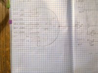
Would a 7430, (NAND) wired to IR3-IR8 followed up by a 7404 (NOT) inverter and that connected to K18, pins 2 an 4 Work ??
I have wired it up with the 7430 and the 7404, and it seems to work fine, on the BreadBoard..
I forgot to draw a Bar over all of the IR's, but they all have that connection..
Also, I may once I hear from Dave, connect the two pins that are connected to +5 to actual IR pins..

001.jpg

I have also done a Variation of the circuit in post 365, instead of using 3 each 2 input NAND's, I have used 2 each 3 input NAND's followed by a 7432 OR followed by a 7404 NOT, which equals a 7402 NOR..
And it seems to work the same as the 7430 circuit..

But what I am finding is that on A4 it is getting it's upper Memory address from the Instruction Register, OR at least it is the same as the Instruction Register.. And not the same as the PC or one more or less than the PC..
And so the program goes into the weeds.. This is on the 6046 instruction, I am not sure if it is also on the 6041 Instruction..
And I am not sure if it has anything to do our circuit or not..

THANK YOU Marty
 
Last edited:
As you have already worked out - your proposal of a 7430 NAND (with the unused inputs tied high) and a 7404 inverter should work beautifully in this circuit. Yep - tie the unused two inputs high via pull-up resistors or tie two inputs back to the same /IRx input. Don't tie more than two inputs to the same /IRx pin - as you will increase the loading on that specific /IRx pin more than the others.

Not sure about what you are getting at regarding your last paragraph - but if you send me a 'trace dump' of your PDP-8 registers just around that point I am sure it will become clear. Let's shake the bugs out one at a time as always... There did seem to be an issue with the original schematics around using the PC or the MA register. I will dig out my old notes and refresh my memory in the meantime (your problem may have something to do with this). This problem is in the effective address calculation area.

Dave
 
Just refreshed my memory...

In the original schematics - the Effective Address was computed as follows:

EA0-4 = PC0-4 providing IR4=1 otherwise EA0-4 = 00000;

EA5-11 = IR5-11;

This had a problem in that during the FETCH cycle, the PC is incremented ***BEFORE*** it is used in the determination of the Effective Address. Therefore, an attempt to perform a memory operation when we were just about to traverse a page boundary would have failed (I proved this to myself as I had implemented the original schematics and made a note to myself that I thought this looked wrong - and I was proved right).

During an even earlier cycle of the FETCH state machine, the PC register is transferred to MA the register to be used as the address of the instruction *** BEFORE *** the PC is incremented. In my LOGISIM simulation I changed PC0-4 to MA0-4 and everything worked as expected across page boundaries i.e. the EA logic I implemented is:

EA0-4 = MA0-4 providing IR4=1 otherwise EA0-4 = 00000;

EA5-11 = IR5-11;

This may not be your problem of course - I am just guessing.

The logic to check is on schematic LD18. Where are G4 pin 2 and G3 pins 13, 10, 5 and 2 wired to on your implementation? If they are wired to The PC register (F2) then this is potentially incorrect. They should be wired to the MA register (F13?).

Dave
 
Hi All;

Dave, Thank You for Your input..

I hope You had a Great and Blessed Christmas..

"" Let's shake the bugs out one at a time as always... ""

""This may not be your problem of course - I am just guessing.

"" EA0-4 = MA0-4 providing IR4=1 otherwise EA0-4 = 00000;
EA5-11 = IR5-11; ""

I think this is working fine, YET, this is Part of the problem..
On a 6XXX Instruction, XXX should not be part of the MA Address , but the address of the I/O Port..
IF I UnderStand this Correctly.. And I don't know where this address is stored or if it should be stored..
But, It should not go to the MA at this time..

I Just did some Reading of State 4, and so, I know at least where to look for a Problem,
(( IOT + MIC + (JMS + JMP + DCA) . IR3 = 1.. ))
K16.6 , M11.6 , G10.12 , K15.6 ..
Of course, in mine they are different numbers, but the same logic.. Maybe it's a Bad IC.. I can follow it thru.. And Monitor J7.4..
IF, I follow the Logic J7, pin 4 should be a low for IOT at K15.6, and High at other times..
I can put this on the BreadBoard, Maybe something will shake out..

The logic to check is on schematic LD18. Where are G4 pin 2 and G3 pins 13, 10, 5 and 2 wired to on your implementation? If they are wired to The PC register (F2) then this is potentially incorrect. They should be wired to the MA register (F13?). ""

This is where I tied my lines, (MA) But, let me check for sure my wiring connections..

THANK YOU Marty
 
Last edited:
You may be confusing yourself as the FETCH state machine may not be doing what you think...

State F0 - The PC is transferred to MA and a read cycle initiated to pickup the instruction from memory.
State F1 - The instruction just read from memory in state F0 is stored into IR.
State F2 - The PC is incremented once to point to the next sequential instruction.
State F3 - The effective address (EA) is calculate and stored into MA *** EVEN IF THE INSTRUCTION IS AN IOT (6XXX) ***
State F4 - If the instruction was an OPR or an IOT or a DIRECT JMP or JMS or DCA then 'bail out' by going to A4 (transfer to EXECUTE cycle).

So, An IOT instruction in IR (6XXX) (or an OPR instruction (7XXX) for that matter) will end up effectively 'corrupting' MA as a consequence of state F3. An OPR or IOT doesn't require a memory address - so the EXECUTE cycle just ignores MA... A direct JMP, JMS or DCA instruction will require the memory address stored in MA.

Does this explanation fit with what you are seeing?

Dave
 
Hi All;

Dave, Thank You for this Fabulous Explanation..

"" You may be confusing yourself as the FETCH state machine may not be doing what you think... ""
It wouldn't be a first time..

"" State F0 - The PC is transferred to MA and a read cycle initiated to pickup the instruction from memory.
State F1 - The instruction just read from memory in state F0 is stored into IR.
State F2 - The PC is incremented once to point to the next sequential instruction.
State F3 - The effective address (EA) is calculate and stored into MA *** EVEN IF THE INSTRUCTION IS AN IOT (6XXX) ***
State F4 - If the instruction was an OPR or an IOT or a DIRECT JMP or JMS or DCA then 'bail out' by going to A4 (transfer to EXECUTE cycle). ""

I'LL have to check for sure and Report back..

"" So, An IOT instruction in IR (6XXX) (or an OPR instruction (7XXX) for that matter) will end up effectively 'corrupting' MA as a consequence of state F3. ""
"" An OPR or IOT doesn't require a memory address - so the EXECUTE cycle just ignores MA... ""
I am not sure If it is being ignored, I will check for sure..

"" A direct JMP, JMS or DCA instruction will require the memory address stored in MA. ""
Yes..

Does this explanation fit with what you are seeing? ""

I'LL have to check for sure and Report back..

I'm going to check my logic since I have it on the BreadBoard, anyway..
So, far it looks OK..

THANK YOU Marty
 
Last edited:
Hi All;

Dave, I think Everything is working fine..

I maybe have another problem, I don't think it is in the main Board..
But, it could be in the I/O part of the machine..
I want to make sure of two things..
1. That I have it wired correctly, for TTY Output, for now, later we can worry about TTY Input..
2. That my program is correct..
So, I want to know once I show You a basic program, how to finish it up, so that It works over and over..
I have proved that I can Output to the Uart, What I am not sure of is 'if' the Flag part of it, is completely working..

0000 7200 CLA
0001 6046 TLS "Initialize the I/O"..
0002 7000 NOOP "Just in case I need to insert something"..
0003 1020 TAD 20 "Where I put my 'A' ..
0004 6046 TLS "output 'A'..
Between here..
0005 7000 NOOP "Just in case I need to insert something"..
0006 6041 TSF Skip if Flag is 1..
0007 5006 JMP 0006
And here it never gets to 0010
0010 7000 NOOP "Just in case I need to insert something"..
0011 5003 JMP to TAD

0020 0101 "A"...

This program will Print the Initial 'A', but then it Loops between 0006 and 0007..
Any Ideas ??
Or is my Program wrong between the two 'here's..

I am going to put the 7474 on the BreadBoard, and put Set (6040) and Reset (6042) in the Instruction Register and see if it does or not..
There is No 6040 Instruction, but there is a 6042 instruction..
So, I am going to try and implement it..

THANK YOU Marty
 
Last edited:
I can't see anything immediately wrong with your test program.

The following test descriptions refer to document "TTY interface.pdf".

The first thing to get working correctly is the "IOP generator" detailed on figure 1 (IC G20).

Enter the following short program and RUN it:

0000 6420 IOT "no device" 0.
0001 5000 JMP 0

Check G20 pins 12, 6 and 8 - they should always be '1'.

Change address 0000 to be 6421 and re-run the program.

Check G20 pin 12 (IOP1.L) goes low during CP0 and the other G20 output pins (6 and 8) remain at '1'.

Change address 0000 to be 6422 and re-run the program.

Check G20 pin 6 (IOP2.L) goes low during CP1 and the other G20 output pins (12 and 8) remain at '1'.

Change address 0000 to be 6424 and re-run the program.

Check G20 pin 8 (IOP4.L) goes low during CP2 and the other G20 output pins (12 and 6) remain at '1'.

Change address 0000 to be 6427 and re-run the program.

Check G20 pin 12 (IOP1.L) goes low during CP0.
Check G20 pin 6 (IOP2.L) goes low during CP1.
Check G20 pin 8 (IOP4.L) goes low during CP2.

If something is wrong with the above - the I/O sub-system will not work properly!

Dave
 
Next, enter the following noddy program and RUN.

0000 6042 IOT TTY_OUT 2 (TCF - Clear Teleprinter flag).
0001 5000 JMP 0

You should see a low going pulse on E20 pin 1 (figure 2 of document "TTY interface.pdf") during CP1. E20 pin 5 (Q output) should be cleared to a logic '0'.

Dave
 
Looking at figure 2 of "TTY interface.pdf" and the 6402 UART data sheet at https://www.intersil.com/content/dam/Intersil/documents/hd-6/hd-6402.pdf on page 5 - pin 22 of the UART (TBRE) should go LOW when a character is loaded into the UART (pin 23 /TBRL goes from high to low then high again) and will go high again when the character has been transferred to the transmit register. The act of going from '0' to '1' should set the 7474 flip-flop flag E20 pin 5 (Q) to a '1'. Try this noddy program:

Load up AC with your desired character to output prior to hitting CONT.

0000 6046 TLS (Teleprinter load and start) - Should reset our E20 pin 5 flip-flop flag and send whatever is in AC to the UART.
0000 7402 HLT

On the scope you should see E20 pin 1 (clear flip-flop flag) pulse low during CP1.

You should also see pin 23 of the UART pulse low (data to UART) during CP2.

You should see pin 22 of the UART go from '1' to '0' when the data is loaded into the UART and then '0' to '1' shortly later as the data starts to squirt out of the UART transmit pin.

You should then see E20 pin 5 go from '0' to '1' signifying that the UART transmit buffer is now free again. This will (however) happen before the character itself has actually been transmitted - as we are looking at the empty state of the transmit buffer register and not the transmit buffer itself.

You should be able to load AC with a new ASCII value, reset PC back to 0000 and re-run the program to see the chain of events repeat.

If the above works OK - we can then move on to the flag / SKIP processing.

Dave
 
Last edited:
Hi All;

Dave, Thanks for the numerous Postings..

"" Load up AC with your desired character to output prior to hitting CONT.

0000 6046 TLS (Teleprinter load and start) - Should reset our E20 pin 5 flip-flop flag and send whatever is in AC to the UART.
0000 7402 HLT ""

I have in my program done a sort of Similar thing, but I am going to start with what You have posted in #373, and work my way down thru the various tests.. And Let You know How things fair..

And away weee go..

"" The first thing to get working correctly is the "IOP generator" detailed on figure 1 (IC G20).

Enter the following short program and RUN it:

0000 6420 IOT "no device" 0.
0001 5000 JMP 0

Check G20 pins 12, 6 and 8 - they should always be '1'.

I found my First Problem, But an easy fix (I think).. G20 pin 12 is pulsing.. Comparing it with G20 pin 6, I see why..
Time to take a Station Break while I fix this problem..
Fixed .. It was wired to pin 14 instead of pin 15 on the IR Register..

Change address 0000 to be 6421 and re-run the program.

Check G20 pin 12 (IOP1.L) goes low during CP0 and the other G20 output pins (6 and 8) remain at '1'.

YES ..

Change address 0000 to be 6422 and re-run the program.

Check G20 pin 6 (IOP2.L) goes low during CP1 and the other G20 output pins (12 and 8) remain at '1'.

YES ..

Change address 0000 to be 6424 and re-run the program.

Check G20 pin 8 (IOP4.L) goes low during CP2 and the other G20 output pins (12 and 6) remain at '1'.

YES..

Change address 0000 to be 6427 and re-run the program.

Check G20 pin 12 (IOP1.L) goes low during CP0.
Check G20 pin 6 (IOP2.L) goes low during CP1.
Check G20 pin 8 (IOP4.L) goes low during CP2.

YES !!!!

If something is wrong with the above - the I/O sub-system will not work properly! ""

""
Next, enter the following noddy program and RUN.

0000 6042 IOT TTY_OUT 2 (TCF - Clear Teleprinter flag).
0001 5000 JMP 0

You should see a low going pulse on E20 pin 1 (figure 2 of document "TTY interface.pdf") during CP1. E20 pin 5 (Q output) should be cleared to a logic '0'. ""

YES...

"" Looking at figure 2 of "TTY interface.pdf" and the 6402 UART data sheet at https://www.intersil.com/content/dam...-6/hd-6402.pdf on page 5 - pin 22 of the UART (TBRE) should go LOW when a character is loaded into the UART (pin 23 /TBRL goes from high to low then high again) and will go high again when the character has been transferred to the transmit register. The act of going from '0' to '1' should set the 7474 flip-flop flag E20 pin 5 (Q) to a '1'. Try this noddy program:

Load up AC with your desired character to output prior to hitting CONT.

0000 6046 TLS (Teleprinter load and start) - Should reset our E20 pin 5 flip-flop flag and send whatever is in AC to the UART.
0000 7402 HLT

On the scope you should see E20 pin 1 (clear flip-flop flag) pulse low during CP1.

YES..

You should also see pin 23 of the UART pulse low (data to UART) during CP2.

YES

You should see pin 22 of the UART go from '1' to '0' when the data is loaded into the UART and then '0' to '1' shortly later as the data starts to squirt out of the UART transmit pin.

You should then see E20 pin 5 go from '0' to '1' signifying that the UART transmit buffer is now free again. This will (however) happen before the character itself has actually been transmitted - as we are looking at the empty state of the transmit buffer register and not the transmit buffer itself.

You should be able to load AC with a new ASCII value, reset PC back to 0000 and re-run the program to see the chain of events repeat.

YES..

If the above works OK - we can then move on to the flag / SKIP processing. ""

I have entered the following program and NOW it Runs fine, it didn't or wouldn't before..
Fixing the IOP1 did the trick..

0000 7001
0001 6046
0002 6041
0003 5002
0004 5000..

I also, entered the program that I posted above with all of the 7000's in it, and Now it runs, even though the result is not what I expected, it does now work..

Dave, just something to think about, when we get to the Keyboard Input side of things, I will need to Rewire (more than likely) for the other 7474, that You have added into Your Circuit, and I will need to know, What connects to where or who..

I tried 'ECHO' but it is still not working, but at least we got Output to work..

THANK YOU Marty
 
Last edited:
A faulty IOP1 could cause mayhem as the PC would be incorrectly incremented on every IOT 04 instruction (even if you weren't testing the flag).

Does this mean the transmitter is now working correctly or do you need some more test programs (e.g. testing for transmitter interrupt etc.)?

In which case we can move on to the receiver...

This was my test ECHO program (input character from keyboard is echoed back to printer):

0000 6032 KCC - Keyboard clear and read character.
0001 6031 KSF - Keyboard skip if flag set.
0002 5001 JMP 1 - Flag clear therefore keep looping.
0003 6034 KPC - Keyboard flag was set - so something to process. Keyboard read static to AC.
0004 6046 TLS - Teleprinter load and start (clear flag and print character).
0005 6041 TSF - Teleprinter skip if flag set.
0006 5005 JMP 5 - Flag clear therefore keep looping.
0007 5000 JMP 0 - Repeat forever...

With the 6402 UART you won't need my additional 7474 flip-flop as this is effectively internal to the UART (pin 19 of the UART goes high - and stays high - when a received character is available and is cleared by reading the UART).

Dave
 
Last edited:
Hi All;

Dave, Thanks for the next Installment..

"" A faulty IOP1 could cause mayhem as the PC would be incorrectly incremented on every IOT 04 instruction (even if you weren't testing the flag).

Yes, that is what we Found Out !!!!

Does this mean the transmitter is now working correctly

YES !!!!!!!!!!!!!!!!!!!!!!


or do you need some more test programs (e.g. testing for transmitter interrupt etc.)?

I don't know, but we can always come back for these IF it shows we need them..

In which case we can move on to the receiver...

YES..

This was my test ECHO program (input character from keyboard is echoed back to printer):

0000 6032 KCC - Keyboard clear and read character.
0001 6031 KSF - Keyboard skip if flag set.
0002 5001 JMP 1 - Flag clear therefore keep looping.
0003 6034 KPC - Keyboard flag was set - so something to process. Keyboard read static to AC.
0004 6046 TLS - Teleprinter load and start (clear flag and print character).
0005 6041 TSF - Teleprinter skip if flag set.
0006 5005 JMP 5 - Flag clear therefore keep looping.
0007 5000 JMP 0 - Repeat forever...

This is the same one that I tried to use..
I think I used 6036 at address 0003, so I will try 6034.. (Both)..

Which didn't Fly...
It jumps from 0001 to 0002 and back to 0001 (addresses).. Keyboard flag may never get set..

Anything, that I can look at on the UART ?? To see if this is the case or if it is something else..

I have looked at pins 4 and 18 and 19 on the UART and they are all High..

So, some Diagnostic's would be of some Great Help..
Based on what You did before on the Transmitter side, MAYBE I can do the same on the Receiver side of things..

With the 6402 UART you won't need my additional 7474 flip-flop as this is effectively internal to the UART (pin 19 of the UART goes high - and stays high - when a received character is available and is cleared by reading the UART). ""
I am using a COM 2502, I don't know If that makes any difference or Not,
I'LL look and see if I have a 6402.. No..

YES, I have made some progress..

In reverse order,

0000 6034
0001 5000

Run, and I get a pulse at UART pin 4..

0000 6032
0001 5000

Run, and I get a pulse at UART pin 18..

0000 6033
0001 5000

Run, and I get a pulse at E21 pin 5, opposite polarity..


0000 6037
0001 5000

Run, and I get a pulse at UART pin 18, UART pin 4, but NOT on or from UART pin 19, but it is Low and before it was High..
So, Maybe that is correct..

THANK YOU Marty
 
Last edited:
I think I know what is going on. Sorry - a bit of a tease because I have to go and eat lunch :). I will get back to you shortly.

Full marks for doing the set of 'noddy' tests - you have done exactly what I would have done - so you have sped the whole process up.

Back from lunch - the last of the Christmas Pudding used up...

Can you check a couple of things for me please?

1) What is pin 16 of the UART wired to? Is it wired to 0V (in which case this is good) or floating (in which case this is bad). This pin needs to be low to enable the status outputs from the UART. I can't see this pin described on the schematics anywhere (although it is identified as being wired to ground in the wiring schedule). Ditto for UART pin 21 (external reset).

2) What is G17 pin 12 wired to (schematic figure 3)? Is it IR10.H or IR10.L? I suspect you may have it wired to IR10.L - it should be IR10.H.

I agree with most of what you have discovered above:

Instruction 6032 should give you a low-going pulse on UART pin 18 during CP1.
Instruction 6034 should give you a low-going pulse on UART pin 4 during CP2.

Both of these are as you describe them.

The only one I disagree with is instruction 6031 - which should give you a high-going pulse on G17 pin 13 during CP0 (which should be wired to either E21 pin 5 or E31 pin 5 - I can't quite read the writing). You seem to have identified 6033 gives this pulse - which is incorrect. Incidentally, the test program for this should be:

0000 6031 KSF - Keyboard skip on flag set.
0001 5000 JMP 0
0002 5000 JMP 0

The two jumps are there to catch both when it SKIPS and when it doesn't!

If you don't get this behaviour with the 6031 instruction it is probably the IR10 logic level being inverted as I have described above.

Pin 19 of the UART should (normally) be '0'. It will only go to a '1' when a character has been received by the UART (so no amount of playing with the PDP-8 instructions will ever cause this pin to go to a '1').

Pin 19 of the UART should be reset to a '0' (once it has gone to a '1') by the instruction 6032.

From my reading of the schematic the following 603X microcodes are implemented:

4 2 1 (IOP pulses)
1 X X - Read the received character from the UART.
X 1 X - Clear the received data flag.
1 1 X - Read the received character from the UART and clear the received data flag at the same time.
X 0 1 - Skip on received data flag.
1 0 1 - Read the received character from the UART and skip on the received data flag.

What you CAN'T do is 'X 1 1' - Clear the received data flag AND skip on it (this operation seems silly - hence why it is forbidden).

We can (however) force pin 19 of the UART to do what we want by a bit of lateral thinking...

Connect the UARTs transmit line back to the receive line. If you have RS232 buffers installed - then just connect Tx back to Rx. You can also wire Tx to your PC's Rx to see what is being transmitted. What we are going to do is to transmit a known character which should be 'looped-back' to the UART receive side - and we will see what we pick up. Enter the following program:

Set up AC with the character to be transmitted (and what we expect to be received due to the loopback).

0000 6044 TPC - Teleprinter print character.
0001 6032 KCC - Keyboard clear and initiate read of the next character (this should also clear the accumulator).
0002 7200 CLA - Clear accumulator (trash the character to be transmitted - so we don't get confused).
0003 7402 HLT - Halt - to allow time for the character to be transmitted and received via the loopback connector.
0004 6034 KRS - Keyboard read static.
0005 7402 HLT - With received character in the accumulator for inspection. Option to change accumulator value for a different character here.
0006 5000 JMP 0 - Repeat the process again...

Note that instruction 0001 needs to have been completed before the character is transmitted and received - so there is a timing constraint here (i.e. this is a noddy test program and, therefore, may have a few quirks).

If you setup AC with (say) an 'A' character and run the program from location 0000 - you should see the 'A' transmitted and (when the character has been received by the UART) pin 19 on the UART should go from '0' to '1'.

The PDP-8 should HALT. Allow a few milliseconds (for the Tx and Rx!) and hit CONT.

The PDP-8 should halt again with the accumulator showing the same binary pattern as the character you transmitted. If this is the case - this tests the receive data path and we can then concentrate on the receive flag and SKIP.

Dave
 
Last edited:
Hi All;

Dave, Thank You for the Information..

It will be tomorrow, before I can do these Tests, it being Sunday here..

But, I can answer a few questions..

Can you check a couple of things for me please?

1) What is pin 16 of the UART wired to? Is it wired to 0V (in which case this is good) or floating (in which case this is bad). ""
It is wired to LOW..
"" This pin needs to be low to enable the status outputs from the UART. I can't see this pin described on the schematics anywhere (although it is identified as being wired to ground in the wiring schedule). Ditto for UART pin 21 (external reset). ""
It is wired to LOW..

2) What is G17 pin 12 wired to (schematic figure 3)? Is it IR10.H or IR10.L? I suspect you may have it wired to IR10.L - it should be IR10.H.
My copy shows IR10.h, but I will check for sure Tomorrow..
I agree with most of what you have above:

Instruction 6032 should give you a low-going pulse on UART pin 18 during CP1.
Instruction 6034 should give you a low-going pulse on UART pin 4 during CP2.

Both of these are as you describe them.

The only one I disagree with is instruction 6031 - which should give you a high-going pulse on G17 pin 13 during CP0 (which should be wired to either E21 pin 5 or E31 pin 5 - I can't quite read the writing).
It is wired to E21 pin 5..
"" You seem to have identified 6033 gives this pulse - which is incorrect. ""

The reason for this was/is that this signal is derived from IOP1.L Which uses IR11.H and this gate G17 uses IR10..
I Just now see My problem, On one page it shows IR10.L and on the other page I have it as IR10.H ??
I an not sure what I have it connected to , But I strongly suspect that You are Correct, I have it to the wrong pin..
On the copy of the page where I have the rest of the IOP's and I put this as well for a reference, It is labeled as IR10.L and the connection it shows is for the Low connection and G20 pin 6 shows the High connection, So I can rewire it to G20 pin 5, and that will fix it..
I think I know what happened, when I had IOP1 connected to the Wrong pin, then to make this work, it had to be connected to the wrong pin as well..
Which proves two Wrongs Don't make a Right..

Once I get that correct, I bet it will work fine..
Once again it's the seemingly little Bugs that get ME..

Incidentally, the test program for this should be:

0000 6031 KSF - Keyboard skip on flag set.
0001 5000 JMP 0
0002 5000 JMP 0

The two jumps are there to catch both when it SKIPS and when it doesn't!


THANK YOU Marty
 
Last edited:
Back
Top