• Please review our updated Terms and Rules here

Build your own PDP 8I, Part 3..

Hi Marty,

Sorry I have been away - but we are exchanging the boiler control system at our Church and this week as it was the only time to do it. The old one is now out and the new one is in (just) - however we still have at least a days work left yet.

Great to see the progress you are making (especially the one with a load of exclamation marks...)!

The logic modifications I did to include the teletype were the ones described in the PDF document "TTY interface.pdf" - however, I had to make a few changes to the 'glue' logic between the simulation blocks for the teletype and the keyboard under the simulator and the PDP-8 simulation (hence the requirement for the extra 7474 D-type flip-flop that I had).

If you don't wire the teletype and keyboard flags up to the interrupt pin (schematic LD21 gate E5 input pin 12) and pull this input pin to a '0' - then E5 pin 11 should always be a '1' (i.e. no interrupt). You can confirm this on schematic LD11 (J7 pin 8) being a '1' continuously and state A0 never being entered (J5 pin 1 always a '1').

I would also check to make sure that L5 pin 5 (/JMS on schematic LD10) is always a '1'. Also check L8 pin 6 on schematic LD10 whilst you are there - this should always be a '1'.

If any of these are not correct - then JMS instructions are being forced to be decoded and that could account for the corruption of memory location 0000.

Dave
 
Hi All;

Dave, Thank You for taking the time, to give me an answer..

"" but we are exchanging the boiler control system ""
The Boiler Control and Not the whole Boiler, correct..
This should be right up You kind of work, Maybe ???

A Church here in Town about 7-10 years ago, before they had an extensive addition and a Boiler Replacement, (where I helped clean), had a 100 Year Old Boiler, that they were still using, It was originally Coal fired, But had been converted to Gas since then..

"" Great to see the progress you are making (especially the one with a load of exclamation marks...)!

The logic modifications I did to include the teletype were the ones described in the PDF document "TTY interface.pdf" - however, I had to make a few changes to the 'glue' logic between the simulation blocks for the teletype and the keyboard under the simulator and the PDP-8 simulation (hence the requirement for the extra 7474 D-type flip-flop that I had).

If you don't wire the teletype and keyboard flags up to the interrupt pin (schematic LD21 gate E5 input pin 12) and pull this input pin to a '0' - then E5 pin 11 should always be a '1' (i.e. no interrupt). You can confirm this on schematic LD11 (J7 pin 8) being a '1' continuously and state A0 never being entered (J5 pin 1 always a '1').

I would also check to make sure that L5 pin 5 (/JMS on schematic LD10) is always a '1'. Also check L8 pin 6 on schematic LD10 whilst you are there - this should always be a '1'.

If any of these are not correct - then JMS instructions are being forced to be decoded and that could account for the corruption of memory location 0000. ""

It looks like it is doing OK, once I used 6002 IOFF, at the beginning of the program,
But, I will check for sure in a little while..
The MAX232 IC I am using seem to be working fine, Next is hooking it up to my computer, and see IF I can get it to Display an "A"..

For some reason it has gone into the weeds.. I have shut it off, and will return in awhile..

I have gotten "A" 's.. But, at times it goes into the weeds.. But, this at least shows that half of the UART is working..
After wiring up the UART to the RS-232 connector, the computer is behaving better..

001.jpg

No Echo, yet, I still am having to debug that half of the circuit..
But the input IS getting to the UART.. Tomorrow..
I Think I have the answer, It came to me in the middle of the night.. I'LL have to check my wiring, But,
I didn't wire up RDA and RDE back to the main Board..
Here is the Echo program..

0000 6023 KCC
0001 6031 KSF
0002 5001 JMP 1
0003 6034 KPC
0004 6046 TLS
0005 6041 TSF
0006 5005 JMP 5
0007 5000 JMP 0..

I may not have the mnemonics correct, as the program was somewhat blurry..


After that More Input !!!!

THANK YOU Marty
 
Last edited:
Hi All;

No Echo, yet, I still am having to debug that half of the circuit..
But the input IS getting to the UART..

I Think I have the answer, It came to me in the middle of the night.. I'LL have to check my wiring, But,
I didn't wire up RDA and RDE back to the main Board..
Correction, it was wired up to the Expansion plug, and then to the I/O Board, it just wasn't wired from the Expansion plug to the UART.. It is now..

Here is the Echo program..

0000 6032 KCC
0001 6031 KSF
0002 5001 JMP 1
0003 6034 KPC
0004 6046 TLS
0005 6041 TSF
0006 5005 JMP 5
0007 5000 JMP 0..

I may not have the mnemonics correct, as the program was somewhat blurry..

After that More Input !!!!

I have ReEntered the "A" out program, And after single stepping, I found 'A0' does come on..
I am going to need to ReEnter the first part of the program and copy down it's one cycle at a time to Isolate when the 'A0' appears..
"" Also check L8 pin 6 on schematic LD10 whilst you are there - this should always be a '1'. ""
And then it goes to '0'..

Here is the Long Listing..

Start::

MA = 0000
M = 6002
MB = 6002
PC = 0000
IR = 0000
AC = 0000

F0

MA = 0000
M = 6002
MB = 6002
PC = 0000
IR = 0000
AC = 0000

F1

MA = 0000
M = 6002
MB = 6002
PC = 0000
IR = 0000
AC = 0000

F2

MA = 0000
M = 6002
MB = 6002
PC = 0000
IR = 6002
AC = 0000

F3

MA = 0000
M = 6002
MB = 6002
PC = 0001
IR = 6002
AC = 0000

A4

MA = 0002
M = 1020
MB = 6002
PC = 0001
IR = 6002
AC = 0000

CP0

MA = 0002
M = 1020
MB = 6002
PC = 0001
IR = 6002
AC = 0000

Cp1-CP7

MA = 0002
M = 1020
MB = 6002
PC = 0001
IR = 6002
AC = 0000

F0

MA = 0002
M = 1020
MB = 6002
PC = 0001
IR = 6002
AC = 0000

F1

MA = 0001
M = 6044
MB = 6002
PC = 0001
IR = 6002
AC = 0000

F2

MA = 0001
M = 6044
MB = 6002
PC = 0002
IR = 6044
AC = 0000

F3

MA = 0001
M = 6044
MB = 6002
PC = 0002
IR = 6044
AC = 0000

A4

MA = 0044
M = 5062
MB = 6002
PC = 0002
IR = 6044
AC = 0000

CP0

MA = 0044
M = 5062
MB = 6002
PC = 0002
IR = 6044
AC = 0000

Cp1-CP7

MA = 0044
M = 5062
MB = 6002
PC = 0003
IR = 6044
AC = 0000

F0

MA = 0044
M = 5062
MB = 6002
PC = 0003
IR = 6044
AC = 0000

F1

MA = 0003
M = 6041
MB = 6002
PC = 0003
IR = 6044
AC = 0000

F2

MA = 0003
M = 6041
MB = 6002
PC = 0003
IR = 6041
AC = 0000

F3

MA = 0003
M = 6041
MB = 6002
PC = 0004
IR = 6041
AC = 0000

A4

MA = 0003
M = 6041
MB = 6002
PC = 0004
IR = 6041
AC = 0000

F1

MA = 0004
M = 5003
MB = 6002
PC = 0004
IR = 6041
AC = 0000

F2

MA = 0004
M = 5003
MB = 6002
PC = 0004
IR = 5003
AC = 0000

F3

MA = 0004
M = 5003
MB = 6002
PC = 0005
IR = 5003
AC = 0000

A4

MA = 0003
M = 6041
MB = 6002
PC = 0005
IR = 5003
AC = 0000

CP0

MA = 0003
M = 6041
MB = 6002
PC = 0005
IR = 5003
AC = 0000

CP1-7

MA = 0003
M = 6041
MB = 6002
PC = 0003
IR = 5003
AC = 0000


A0

MA = 0000
M = 6002
MB = 6002
PC = 0003
IR = 5003
AC = 0000

CP0

MA = 0000
M = 6002
MB = 6002
PC = 0003
IR = 5003
AC = 0000

Cp1

MA = 0000
M = 7777
MB = 0003
PC = 0003
IR = 5003
AC = 0000

Cp2

MA = 0000
M = 0003
MB = 0003
PC = 0003
IR = 5003
AC = 0000


CP3-CP7

MA = 0000
M = 0003
MB = 0003
PC = 0002 ; This could have been PC = 0001
IR = 5003
AC = 0000

F0

MA = 0000
M = 0003
MB = 0003
PC = 0001
IR = 5003
AC = 0000

F1

MA = 0001
M = 6044
MB = 0003
PC = 0001
IR = 5003
AC = 0000

So, I think we have a problem ?!?!!!

I Ran it again with More Info..

Start:: Faster Clock

MA = 0000
M = 6002
MB = 0000
PC = 0000
IR = 0000
AC = 0000

F0

MA = 0000
M = 0000
MB = 6002
PC = 0000
IR = 0000
AC = 0000

F1

MA = 0000
M = 0000
MB = 6002
PC = 0000
IR = 0000
AC = 0000

F2

MA = 0000
M = 6002
MB = 0000
PC = 0000
IR = 6002
AC = 0000

F3

MA = 0000
M = 6002
MB = 0000
PC = 0001
IR = 6002
AC = 0000

A4

MA = 0002
M = 1020
MB = 0000
PC = 0001
IR = 6002
AC = 0000

CP0

MA = 0002
M = 1020
MB = 0000
PC = 0001
IR = 6002
AC = 0000

Cp1-CP7

MA = 0002
M = 1020
MB = 0000
PC = 0001
IR = 6002
AC = 0000

F0

MA = 0002
M = 1020
MB = 0000
PC = 0001
IR = 6002
AC = 0000

F1

MA = 0001
M = 6044
MB = 0000
PC = 0001
IR = 6002
AC = 0000

F2

MA = 0001
M = 6044
MB = 0000
PC = 0001
IR = 6044
AC = 0000

F3

MA = 0001
M = 6044
MB = 0000
PC = 0002
IR = 6044
AC = 0000

A4

MA = 0044
M = 5062
MB = 0000
PC = 0002
IR = 6044
AC = 0000

CP0

MA = 0044
M = 5062
MB = 0000
PC = 0002
IR = 6044
AC = 0000

Cp1-CP7

MA = 0044
M = 5062
MB = 0000
PC = 0003
IR = 6044
AC = 0000

F0

MA = 0044
M = 5062
MB = 0000
PC = 0003
IR = 6044
AC = 0000

F1

MA = 0003
M = 6041
MB = 0000
PC = 0003
IR = 6044
AC = 0000

F2

MA = 0003
M = 6041
MB = 0000
PC = 0003
IR = 6041
AC = 0000

F3

MA = 0003
M = 6041
MB = 0000
PC = 0004
IR = 6041
AC = 0000

A4

MA = 0003
M = 6041
MB = 0000
PC = 0004
IR = 6041
AC = 0000

F1

MA = 0004
M = 5003
MB = 0000
PC = 0004
IR = 6041
AC = 0000

State = 1000
S0-S3 = 0000
Cin = 1
B1-B4 = 011

F2

MA = 0004
M = 5003
MB = 0000
PC = 0004
IR = 5003
AC = 0000

State = 0100
S0-S3 = 0000
Cin = 1
B1-B4 = 000

F3

MA = 0004
M = 5003
MB = 0000
PC = 0005
IR = 5003
AC = 0000

State = 1100
S0-S3 = 0000
Cin = 1
B1-B4 = 111

A4

MA = 0003
M = 6041
MB = 0000
PC = 0005
IR = 5003
AC = 0000

State = 0010
S0-S3 = 0000
Cin = 1
B1-B4 = 000

CP0

MA = 0003
M = 6041
MB = 0000
PC = 0005
IR = 5003
AC = 0000

State = 0010
S0-S3 = 0000
Cin = 1
B1-B4 = 010


CP1-7

MA = 0003
M = 6041
MB = 0000
PC = 0003
IR = 5003
AC = 0000

State = 0000
S0-S3 = 0000
Cin = 1
B1-B4 = 000


A0

MA = 0000
M = 6002
MB = 0000
PC = 0003
IR = 5003
AC = 0000

State = 0000
S0-S3 = 0000
Cin = 1
B1-B4 = 000

CP0

MA = 0000
M = 6002
MB = 0000
PC = 0003
IR = 5003
AC = 0000

State = 0000
S0-S3 = 0000
Cin = 1
IE = 1
B1-B4 = 000

Cp1

MA = 0000
M = 7777
MB = 0003
PC = 0003
IR = 5003
AC = 0000

State = 0000
S0-S3 = 0000
Cin = 1
IE = 1
B1-B4 = 000

Cp2

MA = 0000
M = 0003
MB = 0003
PC = 0003
IR = 5003
AC = 0000

State = 0000
S0-S3 = 0000
Cin = 0
IE = 1
B1-B4 = 010


CP3-CP7

MA = 0000
M = 0003
MB = 0003
PC = 0002
IR = 5003
AC = 0000

State = 0000
S0-S3 = 0000
Cin = 1
IE = 1
B1-B4 = 000

F0

MA = 0000
M = 0003
MB = 0003
PC = 0001
IR = 5003
AC = 0000

State = 0000
S0-S3 = 0000
Cin = 0
IE = 1
B1-B4 = 000

F1

MA = 0001
M = 6044
MB = 0003
PC = 0002
IR = 5003
AC = 0000

State = 1000
S0-S3 = 0000
Cin = 1
IE = 1
B1-B4 = 011

F2

MA = 0001
M = 6044
MB = 0003
PC = 0002
IR = 5003
AC = 0000

State = 0100
S0-S3 = 0000
Cin = 0
IE = 1
B1-B4 = 000

F3

MA = 0001
M = 6044
MB = 0003
PC = 0002
IR = 5003
AC = 0000

State = 1100
S0-S3 = 0000
Cin = 1
IE = 1
B1-B4 = 111

A4

MA = 0044
M = 5062
MB = 0003
PC = 0002
IR = 6044
AC = 0000

State = 0010
S0-S3 = 0000
Cin = 1
IE = 1
B1-B4 = 000

CP0

MA = 0044
M = 5062
MB = 0003
PC = 0002
IR = 6044
AC = 0000

State = 0010
S0-S3 = 0000
Cin = 0
IE = 1
B1-B4 = 000

Cp1

MA = 0044
M = 5062
MB = 0003
PC = 0003
IR = 6044
AC = 0000

State = 0000
S0-S3 = 0000
Cin = 1
IE = 1
B1-B4 = 000

CP2

MA = 0044
M = 5062
MB = 0003
PC = 0002
IR = 6044
AC = 0000

State = 0000
S0-S3 = 0111
Mode = 1
Cin = 1
IE = 1
B1-B4 = 001

CP3

MA = 0044
M = 5062
MB = 0003
PC = 0002
IR = 6044
AC = 0000

State = 0000
S0-S3 = 0000
Cin = 1
IE = 1
B1-B4 = 000

F0

MA = 0044
M = 5062
MB = 0003
PC = 0002
IR = 6044
AC = 0000

State = 0000
S0-S3 = 0000
Cin = 1
IE = 1
B1-B4 = 000

Dave, I hope that this Helps ...

Here is another Run, a little Different..

Start:: Faster Clock

MA = 0000
M = 6002
MB = 0000
PC = 0000
IR = 0000
AC = 0000

State = 0000
S3-S0 = 0000
Cin = 1
IE = 1
B1-B4 000

F0

MA = 0000
M = 0000
MB = 6002
PC = 0000
IR = 0000
AC = 0000

State = 0000
S3-S0 = 0000
Cin = 1
IE = 1
B1-B4 000

F1

MA = 0000
M = 0000
MB = 6002
PC = 0000
IR = 0000
AC = 0000

State = 1000
S3-S0 = 0000
Cin = 1
IE = 1
B1-B4 011

F2

MA = 0000
M = 6002
MB = 0000
PC = 0000
IR = 6002
AC = 0000

State = 0100
S3-S0 = 0000
Cin = 0
IE = 1
B1-B4 000

F3

MA = 0000
M = 6002
MB = 0000
PC = 0001
IR = 6002
AC = 0000

State = 1100
S3-S0 = 0000
Cin = 1
IE = 1
B1-B4 111

A4

MA = 0002
M = 1020
MB = 0000
PC = 0001
IR = 6002
AC = 0000

State = 0010
S3-S0 = 0000
Cin = 1
IE = 1
B1-B4 000

CP0

MA = 0002
M = 1020
MB = 0000
PC = 0001
IR = 6002
AC = 0000

State = 0010
S3-S0 = 0000
Cin = 0
IE = 1
B1-B4 000


Cp1

MA = 0002
M = 1020
MB = 0000
PC = 0001
IR = 6002
AC = 0000

State = 0000
S3-S0 = 0000
Cin = 1
IE = 1
B1-B4 000

Cp2

MA = 0002
M = 1020
MB = 0000
PC = 0001
IR = 6002
AC = 0000

State = 0000
S3-S0 = 0111
Mode = 1
Cin = 1
IE = 1
B1-B4 001

CP3

MA = 0002
M = 1020
MB = 0000
PC = 0001
IR = 6002
AC = 0000

State = 0000
S3-S0 = 0000
Mode = 0
Cin = 1
IE = 1
B1-B4 000

F0

MA = 0002
M = 1020
MB = 0000
PC = 0001
IR = 6002
AC = 0000

State = 0000
S3-S0 = 0000
Mode = 0
Cin = 1
IE = 1
B1-B4 000

F1

MA = 0001
M = 6044
MB = 0000
PC = 0001
IR = 6002
AC = 0000

State = 1000
S3-S0 = 0000
Mode = 0
Cin = 1
IE = 1
B1-B4 011

F2

MA = 0001
M = 6044
MB = 0000
PC = 0001
IR = 6044
AC = 0000

State = 0100
S3-S0 = 0000
Mode = 0
Cin = 0
IE = 1
B1-B4 000

F3

MA = 0001
M = 6044
MB = 0000
PC = 0002
IR = 6044
AC = 0000

State = 1100
S3-S0 = 0000
Mode = 0
Cin = 1
IE = 1
B1-B4 111

A4

MA = 0044
M = 5062
MB = 0000
PC = 0002
IR = 6044
AC = 0000

State = 0010
S3-S0 = 0000
Mode = 0
Cin = 1
IE = 1
B1-B4 000

CP0

MA = 0044
M = 5062
MB = 0000
PC = 0002
IR = 6044
AC = 0000

State = 0010
S3-S0 = 0000
Mode = 0
Cin = 0
IE = 1
B1-B4 000

Cp1

MA = 0044
M = 5062
MB = 0000
PC = 0003
IR = 6044
AC = 0000

State = 0000
S3-S0 = 0000
Mode = 0
Cin = 1
IE = 1
B1-B4 000

CP2

MA = 0044
M = 5062
MB = 0000
PC = 0003
IR = 6044
AC = 0000

State = 0000
S3-S0 = 0111
Mode = 1
Cin = 1
IE = 1
B1-B4 001

Cp3-CP7

MA = 0044
M = 5062
MB = 0000
PC = 0003
IR = 6044
AC = 0000

State = 0000
S3-S0 = 0000
Mode = 0
Cin = 1
IE = 1
B1-B4 000

F0

MA = 0044
M = 5062
MB = 0000
PC = 0003
IR = 6044
AC = 0000

State = 0000
S3-S0 = 0000
Mode = 0
Cin = 1
IE = 1
B1-B4 000

F1

MA = 0003
M = 6041
MB = 0000
PC = 0003
IR = 6044
AC = 0000

State = 1000
S3-S0 = 0000
Mode = 0
Cin = 1
IE = 1
B1-B4 011

F2

MA = 0003
M = 6041
MB = 0000
PC = 0003
IR = 6041
AC = 0000

State = 0100
S3-S0 = 0000
Mode = 0
Cin = 0
IE = 1
B1-B4 000

F3

MA = 0003
M = 6041
MB = 0000
PC = 0004
IR = 6041
AC = 0000

State = 0000
S3-S0 = 0000
Mode = 0
Cin = 1
IE = 1
B1-B4 000

A4

MA = 0003
M = 6041
MB = 0000
PC = 0004
IR = 6041
AC = 0000

State = 1100
S3-S0 = 0000
Mode = 0
Cin = 1
IE = 1
B1-B4 000

F1

MA = 0004
M = 5003
MB = 0000
PC = 0004
IR = 6041
AC = 0000

State = 1000
S0-S3 = 0000
Mode = 0
Cin = 1
B1-B4 = 011

F2

MA = 0004
M = 5003
MB = 0000
PC = 0004
IR = 5003
AC = 0000

State = 0100
S0-S3 = 0000
Mode = 0
Cin = 1
B1-B4 = 000

F3

MA = 0004
M = 5003
MB = 0000
PC = 0005
IR = 5003
AC = 0000

State = 1100
S0-S3 = 0000
Cin = 1
B1-B4 = 111

A4

MA = 0003
M = 6041
MB = 0000
PC = 0005
IR = 5003
AC = 0000

State = 0010
S0-S3 = 0000
Cin = 1
B1-B4 = 000

CP0

MA = 0003
M = 6041
MB = 0000
PC = 0005
IR = 5003
AC = 0000

State = 0010
S0-S3 = 0000
Cin = 1
B1-B4 = 010


CP1-7

MA = 0003
M = 6041
MB = 0000
PC = 0003
IR = 5003
AC = 0000

State = 0000
S0-S3 = 0000
Cin = 1
B1-B4 = 000


A0

MA = 0000
M = 6002
MB = 0000
PC = 0003
IR = 5003
AC = 0000

State = 0000
S0-S3 = 0000
Cin = 1
B1-B4 = 000

CP0

MA = 0000
M = 6002
MB = 0000
PC = 0003
IR = 5003
AC = 0000

State = 0000
S0-S3 = 0000
Cin = 1
IE = 1
B1-B4 = 000

Cp1

MA = 0000
M = 7777
MB = 0003
PC = 0003
IR = 5003
AC = 0000

State = 0000
S0-S3 = 0000
Cin = 1
IE = 1
B1-B4 = 000

Cp2

MA = 0000
M = 0003
MB = 0003
PC = 0003
IR = 5003
AC = 0000

State = 0000
S0-S3 = 0000
Cin = 0
IE = 1
B1-B4 = 010


CP3-CP7

MA = 0000
M = 0003
MB = 0003
PC = 0002
IR = 5003
AC = 0000

State = 0000
S0-S3 = 0000
Cin = 1
IE = 1
B1-B4 = 000

F0

MA = 0000
M = 0003
MB = 0003
PC = 0001
IR = 5003
AC = 0000

State = 0000
S0-S3 = 0000
Cin = 1
IE = 1
B1-B4 = 000

F1

MA = 0001
M = 6044
MB = 0003
PC = 0001
IR = 5003
AC = 0000

State = 1000
S0-S3 = 0000
Cin = 1
IE = 1
B1-B4 = 011

F2

MA = 0001
M = 6044
MB = 0003
PC = 0001
IR = 6044
AC = 0000

State = 0100
S0-S3 = 0000
Cin = 0
IE = 1
B1-B4 = 000

F3

MA = 0001
M = 6044
MB = 0003
PC = 0002
IR = 6044
AC = 0000

State = 1100
S0-S3 = 0000
Cin = 1
IE = 1
B1-B4 = 111

A4

MA = 0044
M = 5062
MB = 0003
PC = 0002
IR = 6044
AC = 0000

State = 0010
S0-S3 = 0000
Cin = 1
IE = 1
B1-B4 = 000

CP0

MA = 0044
M = 5062
MB = 0003
PC = 0002
IR = 6044
AC = 0000

State = 0010
S0-S3 = 0000
Cin = 0
IE = 1
B1-B4 = 000

Cp1

MA = 0044
M = 5062
MB = 0003
PC = 0003
IR = 6044
AC = 0000

State = 0000
S0-S3 = 0000
Cin = 1
IE = 1
B1-B4 = 000

CP2

MA = 0044
M = 5062
MB = 0003
PC = 0003
IR = 6044
AC = 0000

State = 0000
S0-S3 = 0111
Mode = 1
Cin = 1
IE = 1
B1-B4 = 001

CP3

MA = 0044
M = 5062
MB = 0003
PC = 0003
IR = 6044
AC = 0000

State = 0000
S0-S3 = 0000
Cin = 1
IE = 1
B1-B4 = 000

F0

MA = 0044
M = 5062
MB = 0003
PC = 0003
IR = 6044
AC = 0000

State = 0000
S0-S3 = 0000
Cin = 1
IE = 1
B1-B4 = 000

F1

MA = 0003
M = 6044
MB = 0003
PC = 0003
IR = 6044
AC = 0000

State = 1000
S0-S3 = 0000
Cin = 1
IE = 1
B1-B4 = 011

F2

MA = 0003
M = 6044
MB = 0003
PC = 0003
IR = 6044
AC = 0000

State = 0100
S0-S3 = 0000
Cin = 0
IE = 1
B1-B4 = 000

F3

MA = 0003
M = 6044
MB = 0003
PC = 0003
IR = 6044
AC = 0000

State = 0100
S0-S3 = 0000
Cin = 0
IE = 1
B1-B4 = 000

A4

MA = 0003
M = 6044
MB = 0003
PC = 0004
IR = 6044
AC = 0000

State = 1100
S0-S3 = 0000
Cin = 1
IE = 1
B1-B4 = 000

F1

MA = 0004
M = 5003
MB = 0003
PC = 0004
IR = 6044
AC = 0000

State = 1000
S0-S3 = 0000
Cin = 0
IE = 1
B1-B4 = 011

F2

MA = 0004
M = 5003
MB = 0003
PC = 0004
IR = 5003
AC = 0000

State = 0100
S0-S3 = 0000
Cin = 0
IE = 0
B1-B4 = 000


F3

MA = 0004
M = 5003
MB = 0003
PC = 0005
IR = 5003
AC = 0000

State = 1100
S0-S3 = 0000
Cin = 0
IE = 1
B1-B4 = 111

A4

MA = 0003
M = 6041
MB = 0003
PC = 0005
IR = 5003
AC = 0000

State = 0010
S0-S3 = 0000
Cin = 1
IE = 0
B1-B4 = 000

CP0

MA = 0003
M = 6041
MB = 0003
PC = 0005
IR = 5003
AC = 0000

State = 0010
S0-S3 = 0000
Cin = 1
IE = 0
B1-B4 = 010

CP1

MA = 0003
M = 6041
MB = 0003
PC = 0003
IR = 5003
AC = 0000

State = 0000
S0-S3 = 0000
Cin = 1
IE = 0
B1-B4 = 000

CP2

MA = 0003
M = 6041
MB = 0003
PC = 0003
IR = 5003
AC = 0000

State = 0000
S0-S3 = 0000
Cin = 1
IE = 0
B1-B4 = 000

A0

MA = 0000
M = 0003
MB = 0003
PC = 0003
IR = 5003
AC = 0000

State = 0000
S0-S3 = 0000
Cin = 1
IE = 0
B1-B4 = 000

CP0

MA = 0000
M = 0003
MB = 0003
PC = 0003
IR = 5003
AC = 0000

State = 0000
S0-S3 = 0000
Cin = 1
IE = 1
B1-B4 = 000

CP1

MA = 0000
M = 0003
MB = 0003
PC = 0003
IR = 5003
AC = 0000

State = 0000
S0-S3 = 0000
Cin = 1
IE = 1
B1-B4 = 000

CP2-CP7

MA = 0000
M = 0003
MB = 0003
PC = 0003
IR = 5003
AC = 0000

State = 0000
S0-S3 = 0000
Cin = 1
IE = 1
B1-B4 = 010

F0

MA = 0000
M = 0003
MB = 0003
PC = 0001
IR = 5003
AC = 0000

State = 0000
S0-S3 = 0000
Cin = 1
IE = 1
B1-B4 = 000

Dave, take the best match of two of three or what makes the best sense..

THANK YOU Marty
 
Last edited:
Marty,

There is something not making sense somewhere (I state the obvious). Can you list your program please that you are using.

In the first case, instruction 6002 is being loaded from memory location 0000. This instruction (technically) doesn't exist in this machine and should behave as an IOF (interrupt OFF). So where is the interrupt coming from to force state A0?

On schematic LD21, E14 pin 9 should always be a '0'.

You are remembering to press CLEAR before loading up the registers to RUN aren't you? The clear pulse should reset E14 pin 9 (via E14 pin 13 pulsing low) and then E14 pin 9 should never get set again.

If E14 pin 9 is always a '0', this means E5 pin 13 should always be a '0' (it is the same piece of wire) and (therefore) it shouldn't matter what interrupts are generated by the UART on E5 pin 12. E5 pin 11 should always be a '1' by the action of E5 pin 13 always being a '0'.

If the above makes sense...

Dave
 
Hi Alll

Dave, Thank You for Your Answer, I went to the Store and Just got back..

"" There is something not making sense somewhere (I state the obvious). ""
YES !!!
"" Can you list your program please that you are using. ""

Yes, I thought I listed Earlier..
0000 6002 IOFF (I Thought) I will change this to 6000 for my next Run..
0001 6044 TPC
0002 1020 TAD 20
0003 6041 TSF
0004 5003 JMP 03
0005 6046 TLS
0006 5002 JMP 02..

0020 0101 'A'

"" This instruction (technically) doesn't exist in this machine and should behave as an IOF (interrupt OFF). ""
So, What is the correct Instruction for IOFF ?? And I will Change my Code.. I Found it 6000 IOFF..

"" On schematic LD21, E14 pin 9 should always be a '0'. ""
I will Monitor this, and see IF I can find out or see when it Changes.. Hopefully, Pinpoint the trouble..

"" You are remembering to press CLEAR before loading up the registers to RUN aren't you? ""
YES !!!
"" If E14 pin 9 is always a '0', this means E5 pin 13 should always be a '0' (it is the same piece of wire) and (therefore) it shouldn't matter what interrupts are generated by the UART on E5 pin 12. E5 pin 11 should always be a '1' by the action of E5 pin 13 always being a '0'.

If the above makes sense... ""
YES !!!

I will Re-Run it and Monitor E14, pin 9..

THANK YOU Marty
 
Last edited:
Hi All;

DAVE, I FOUND IT !!!!

You'LL probably tell me it's at A4 instead of F1,
so look at Both.. Or even the whole area..
Tomorrow, I will put the original ION/IOFF circuit on the BreadBoard,
And see if that is the problem, after that I will put the rest of Interrupt circuit
on the BreadBoard and check that as well..
Hopefully, something somewhere will show up..
I just checked, looking/thinking, I had miswired, K18.11 to A4 instead of A3..
But, that is not the case, I checked both A3 and A4 with a beeing meter, And it has A3 wired to it..
Now I'm going to wire the interrupt circuitry on the BreadBoard, and see if it still shows the same thing..

Start:: Faster Clock

MA = 0000
M = 6000
MB = 0000
PC = 0000
IR = 0000
AC = 0000

State = 0000
S3-S0 = 0000
Cin = 1
IE = 1
B1-B4 000
E14, 9 = 0

F0

MA = 0000
M = 6000
MB = 0000
PC = 0000
IR = 0000
AC = 0000

State = 0000
S3-S0 = 0000
Cin = 1
IE = 1
B1-B4 000
E14, 9 = 0

F1

MA = 0000
M = 6000
MB = 0000
PC = 0000
IR = 0000
AC = 0000

State = 1000
S3-S0 = 0000
Cin = 1
IE = 1
B1-B4 011
E14, 9 = 0

F2

MA = 0000
M = 6000
MB = 0000
PC = 0000
IR = 6000
AC = 0000

State = 0100
S3-S0 = 0000
Cin = 0
IE = 1
B1-B4 000
E14, 9 = 0

F3

MA = 0000
M = 6000
MB = 0000
PC = 0001
IR = 6000
AC = 0000

State = 1100
S3-S0 = 0000
Cin = 1
IE = 1
B1-B4 111
E14, 9 = 0

A4

MA = 0000
M = 1020
MB = 0000
PC = 0001
IR = 6000
AC = 0000

State = 0010
S3-S0 = 0000
Cin = 1
IE = 1
B1-B4 000
E14, 9 = 0

CP0

MA = 0000
M = 6000
MB = 0000
PC = 0001
IR = 6000
AC = 0000

State = 0010
S3-S0 = 0000
Cin = 0
IE = 1
B1-B4 000
E14, 9 = 0

Cp1

MA = 0000
M = 6000
MB = 0000
PC = 0001
IR = 6000
AC = 0000

State = 0000
S3-S0 = 0000
Cin = 1
IE = 1
B1-B4 000
E14, 9 = 0

Cp2

MA = 0000
M = 6000
MB = 0000
PC = 0001
IR = 6000
AC = 0000

State = 0000
S3-S0 = 0111
Mode = 1
Cin = 1
IE = 1
B1-B4 001
E14, 9 = 0

CP3

MA = 0000
M = 6000
MB = 0000
PC = 0001
IR = 6000
AC = 0000

State = 0000
S3-S0 = 0000
Mode = 0
Cin = 1
IE = 1
B1-B4 000
E14, 9 = 0

F0

MA = 0000
M = 6000
MB = 0000
PC = 0001
IR = 6000
AC = 0000

State = 0000
S3-S0 = 0000
Mode = 0
Cin = 1
IE = 1
B1-B4 000
E14, 9 = 0

F1

MA = 0001
M = 6044
MB = 0000
PC = 0001
IR = 6000
AC = 0000

State = 1000
S3-S0 = 0000
Mode = 0
Cin = 1
IE = 1
B1-B4 011
E14, 9 = 0

F2

MA = 0001
M = 6044
MB = 0000
PC = 0001
IR = 6044
AC = 0000

State = 0100
S3-S0 = 0000
Mode = 0
Cin = 0
IE = 1
B1-B4 000
E14, 9 = 0

F3

MA = 0001
M = 6044
MB = 0000
PC = 0002
IR = 6044
AC = 0000

State = 1100
S3-S0 = 0000
Mode = 0
Cin = 1
IE = 1
B1-B4 111
E14, 9 = 0

A4

MA = 0044
M = 5062
MB = 0000
PC = 0002
IR = 6044
AC = 0000

State = 0010
S3-S0 = 0000
Mode = 0
Cin = 1
IE = 1
B1-B4 000
E14, 9 = 0

CP0

MA = 0044
M = 5062
MB = 0000
PC = 0002
IR = 6044
AC = 0000

State = 0010
S3-S0 = 0000
Mode = 0
Cin = 0
IE = 1
B1-B4 000
E14, 9 = 0

Cp1

MA = 0044
M = 5062
MB = 0000
PC = 0003
IR = 6044
AC = 0000

State = 0000
S3-S0 = 0000
Mode = 0
Cin = 1
IE = 1
B1-B4 000
E14, 9 = 0

CP2

MA = 0044
M = 5062
MB = 0000
PC = 0003
IR = 6044
AC = 0000

State = 0010
S3-S0 = 0111
Mode = 1
Cin = 1
IE = 1
B1-B4 001
E14, 9 = 0

Cp3-CP7

MA = 0044
M = 5062
MB = 0000
PC = 0003
IR = 6044
AC = 0000

State = 0000
S3-S0 = 0000
Mode = 0
Cin = 1
IE = 1
B1-B4 000
E14, 9 = 0

F0

MA = 0044
M = 5062
MB = 0000
PC = 0003
IR = 6044
AC = 0000

State = 0000
S3-S0 = 0000
Mode = 0
Cin = 1
IE = 1
B1-B4 000
E14, 9 = 0

F1

MA = 0003
M = 6041
MB = 0000
PC = 0003
IR = 6044
AC = 0000

State = 1000
S3-S0 = 0000
Mode = 0
Cin = 1
IE = 1
B1-B4 011
E14, 9 = 0

F2

MA = 0003
M = 6041
MB = 0000
PC = 0003
IR = 6041
AC = 0000

State = 0100
S3-S0 = 0000
Mode = 0
Cin = 0
IE = 1
B1-B4 000
E14, 9 = 0

F3

MA = 0003
M = 6041
MB = 0000
PC = 0004
IR = 6041
AC = 0000

State = 0000
S3-S0 = 0000
Mode = 0
Cin = 1
IE = 1
B1-B4 000
E14, 9 = 0

A4

MA = 0003
M = 6041
MB = 0000
PC = 0004
IR = 6041
AC = 0000

State = 1100
S3-S0 = 0000
Mode = 0
Cin = 1
IE = 1
B1-B4 000
E14, 9 = 0

F1 HERE !!!!!!!!!!!!!!!!!!!!!!!!!!!!!!!!!!!!!!!!!!!!!!!!!!!!!!!!!!!!!!!!!!!!!

MA = 0004
M = 5003
MB = 0000
PC = 0004
IR = 6041
AC = 0000

State = 1000
S0-S3 = 0000
Mode = 0
Cin = 1
B1-B4 = 011
E14, 9 = 1 HERE !!!!!!!!!!!!!!!!!!!!!!!!!!!!!!!!!!!!!!!!!!!!!!!!!!!!!!!!!!!!!!!!!!!!!!!!!!!!!!!!!!

F2

MA = 0004
M = 5003
MB = 0000
PC = 0004
IR = 5003
AC = 0000

State = 0100
S0-S3 = 0000
Mode = 0
Cin = 1
B1-B4 = 000
E14, 9 = 1

F3

MA = 0004
M = 5003
MB = 0000
PC = 0005
IR = 5003
AC = 0000

State = 1100
S0-S3 = 0000
Cin = 1
B1-B4 = 111
E14, 9 = 1

A4

MA = 0003
M = 6041
MB = 0000
PC = 0005
IR = 5003
AC = 0000

State = 0010
S0-S3 = 0000
Cin = 1
B1-B4 = 000
E14, 9 = 1

CP0

MA = 0003
M = 6041
MB = 0000
PC = 0005
IR = 5003
AC = 0000

State = 0010
S0-S3 = 0000
Cin = 1
B1-B4 = 010
E14, 9 = 1


CP1-7

MA = 0003
M = 6041
MB = 0000
PC = 0003
IR = 5003
AC = 0000

State = 0000
S0-S3 = 0000
Cin = 1
B1-B4 = 000


A0

MA = 0000
M = 6000
MB = 0000
PC = 0003
IR = 5003
AC = 0000

State = 0000
S0-S3 = 0000
Cin = 1
B1-B4 = 000
E14, 9 = 1

CP0

ETC.,

THANK YOU Marty
 
Last edited:
It's good that you are seeing E14 pin 9 go to a '1' (that accounts for the memory location 0000 getting overwritten and your program going mad) - the question now is why.

The key is going to be on schematic LD21.

The 'top' circuit decodes the value in the IR as 600X - so you should see no low-going pulses on K18 pin 12 (ION.L) or K18 pin 6 (IOF.L). These two pins should always be '1' (unless you execute an ION or IOF = 6001 or 6000 respectively).

Presumably, you will be seeing a '1' on E14 pin 12 (D input) just prior to the clock that causes E14 pin 9 to go from a '0' to a '1'?

The circuitry on the 'lower' half of the schematic is a bit convoluted (to say the least!) and it will take me a short while to remember how this bit works... Will update the post later when I have worked it out again!

Dave
 
Hi All;

Dave, Thank You for Your Insight..

I have the Interrupt on Led's (steroids)..

001.jpg

So, this will show what is actually happening..
"" Presumably, you will be seeing a '1' on E14 pin 12 (D input) just prior to the clock that causes E14 pin 9 to go from a '0' to a '1'? ""
I hope so !!!!

I found the Culprit (A3).. K18, pin 11 !!!!

Start:: Faster Clock
program status starts here..

MA = 0044
M = 5062
MB = 0000
PC = 0003
IR = 6044
AC = 0000

State = 0000
S3-S0 = 0000
Mode = 0
Cin = 1
IE = 1
B1-B4 000

K18.9 = 1
K18.10 = 1
K18.11 = 1
K18.8 = 0

E14, 9 = 0
E14.12 = 0


F0 START Full Info here..

MA = 0044
M = 5062
MB = 0000
PC = 0003
IR = 6044
AC = 0000

State = 0000
S3-S0 = 0000
Mode = 0
Cin = 1
IE = 1
B1-B4 000

K18.9 = 1
K18.10 = 1
K18.11 = 1
K18.8 = 0

E14.11 = 1
E14.12 = 0
E14, 9 = 0

F1

MA = 0003
M = 6041
MB = 0000
PC = 0003
IR = 6044
AC = 0000

State = 1000
S3-S0 = 0000
Mode = 0
Cin = 1
IE = 1
B1-B4 011

K18.9 = 1
K18.10 = 1
K18.11 = 1
K18.8 = 0

E14.11 = 1
E14.12 = 0
E14, 9 = 0

F2

MA = 0003
M = 6041
MB = 0000
PC = 0003
IR = 6041
AC = 0000

State = 0100
S3-S0 = 0000
Mode = 0
Cin = 0
IE = 1
B1-B4 000

K18.9 = 1
K18.10 = 1
K18.11 = 1
K18.8 = 0

E14.11 = 1
E14.12 = 0
E14, 9 = 0

F3 , F3 seems to be skipped
over and it goes to A4..
I noticed this before, but I didn't
take any action.. Just a note..

MA = 0003
M = 6041
MB = 0000
PC = 0004
IR = 6041
AC = 0000

State = 0000
S3-S0 = 0000
Mode = 0
Cin = 1
IE = 1
B1-B4 000

K18.9 = 1
K18.10 = 1
K18.11 = 1
K18.8 = 0

E14.11 = 1
E14.12 = 0
E14, 9 = 0

A4

MA = 0003
M = 6041
MB = 0000
PC = 0004
IR = 6041
AC = 0000

State = 1100
S3-S0 = 0000
Mode = 0
Cin = 1
IE = 1
B1-B4 000

K18.9 = 1
K18.10 = 1
K18.11 = 0 (A3) HERE !!!!!!!!!!!!!!!!!!
K18.8 = 1

E14.11 = 1
E14.12 = 1
E14, 9 = 0

F1

MA = 0004
M = 5003
MB = 0000
PC = 0004
IR = 6041
AC = 0000

State = 1000
S0-S3 = 0000
Mode = 0
Cin = 1
B1-B4 = 011

K18.9 = 1
K18.10 = 1
K18.11 = 1
K18.8 = 0

E14.11 = 1
E14.12 = 1
E14, 9 = 1 HERE !!!!!!!!!!!!!!!!

F2

MA = 0004
M = 5003
MB = 0000
PC = 0004
IR = 5003
AC = 0000

State = 0100
S0-S3 = 0000
Mode = 0
Cin = 1
B1-B4 = 000
E14, 9 = 1

F3

MA = 0004
M = 5003
MB = 0000
PC = 0005
IR = 5003
AC = 0000

State = 1100
S0-S3 = 0000
Cin = 1
B1-B4 = 111
E14, 9 = 1

A4

MA = 0003
M = 6041
MB = 0000
PC = 0005
IR = 5003
AC = 0000

State = 0010
S0-S3 = 0000
Cin = 1
B1-B4 = 000
E14, 9 = 1

CP0

MA = 0003
M = 6041
MB = 0000
PC = 0005
IR = 5003
AC = 0000

State = 0010
S0-S3 = 0000
Cin = 1
B1-B4 = 010
E14, 9 = 1


CP1-7

MA = 0003
M = 6041
MB = 0000
PC = 0003
IR = 5003
AC = 0000

State = 0000
S0-S3 = 0000
Cin = 1
B1-B4 = 000

"" The 'top' circuit decodes the value in the IR as 600X - so you should see no low-going pulses on K18 pin 12 (ION.L) or K18 pin 6 (IOF.L). These two pins should always be '1' (unless you execute an ION or IOF = 6001 or 6000 respectively). ""
Yes, I see that, now.. And so unless it shows that the problem is there, for now, I am leaving it alone..

"" The circuitry on the 'lower' half of the schematic is a bit convoluted (to say the least!) and it will take me a short while to remember how this bit works... ""
Somewhere I remember reading an Explanation of the circuit, Just at present I don't remember where..
I Looked at the Manual, and I Found it.. See below..

Dave, can You run the Diagnostics with K18, pin 11 tied to A3 and K17, pin 5 tied High (1), instead of A3..
And Just the opposite K18, pin 11 tied High and K 17, pin 5 tied to A3..
Thank You..

I Just found 'Why' it is there, Look at State 3 Explanation..
" State 3 is used for processing the Special Instruction ION..
This special command is used to turn the Interrupt system on..
A3, Must reArm the interrupt system, so it Sets 1 --> IE (E14.. ....
Remember that State A0 must turn off the IE Flip-Flop..
During A0, A3 will be High which will apply a low to the D flip-flop E14, pin 12.. ....
During A3 the input to K17, pin 5 will be low, input to D flip-flop will be High..
Thus A3 will Set 1 --> IE..
Explanation of the 7451 circuitry..
As long as the INTLD signal is False, Data from the Flip-flop will be Re-loaded on the next clock Cycle..
If INTLD goes true the old flip-flop output is blocked from the D input and a new signal A3 is Loaded into IE..

I Don't know If this Helps or Hurts, Or if we can find a work around it, like once it is turned OFF, it cannot be turned on by A3..
But, that seems to from the description Defeat the purpose of A3 or multiple Interrupts..

Maybe another solution would be to Tie A3 to K17, pin 5 and to tie K18, pin 11 high..
I Just tried this, and the program Works, No Troublesome Interrupts..
Now, I don't know if or How this might affect multiple Interrupts..

Or, the opposite tie K17, pin 5 High and tie K18, pin 11 to A3..
And this works as well..
Now, I don't know if or How this might affect multiple Interrupts..
Just not Both to A3..
Just a few thoughts..

THANK YOU Marty
 
Last edited:
The problem is that everything is related around here - so you are not sure whether you are seeing the cause or effect or (to put it another way) the chicken or the egg.

You should only be able to get into state A3 by the detection of an ION instruction (schematic LD11 J7 pin 5). But if you don't have any ION instructions (6001) in your program - then how can this occur?

I suspect that 'something' is seeing an ION instruction when one isn't there and (as a result) the state machines are following the correct path for a (phantom) ION instruction.

The place to start is the top schematic of LD21 where ION and IOF are decoded. if your test program doesn't have any ION or IOF instructions then K18 pins 6 and 12 should both be (and stay) high.

If either of these pins go low - then they are only decoding what is in the IR - so what was loaded into the IR at the time when either ION or IOF were decoded?

If these two pins remain at a '1' - then the fault lies elsewhere.

We shouldn't be thinking of 'solutions' until we know exactly what the problem is - and at the moment I don't feel as though we have got to the root cause of the problem - we are just seeing it's effects.

Dave

PS - only one interrupt can occur at a time. When an interrupt occurs - the interrupt flip-flop (E14 pin 9) should be reset. The interrupt handler can (however) re-enable the flip-flop with an ION instruction - it just has to make sure that the return address is preserved from memory location 0000.
 
Hi All;

Dave, Thank You for Your assessment of the problem..

"" I suspect that 'something' is seeing an ION instruction when one isn't there and (as a result) the state machines are following the correct path for a (phantom) ION instruction.

The place to start is the top schematic of LD21 where ION and IOF are decoded. if your test program doesn't have any ION or IOF instructions then K18 pins 6 and 12 should both be (and stay) high.

I will try the program with out an IOFF in it, and Report the effects back to You, I will Monitor Both of the pins.. ( K18 pins 6 and 12)..

I am going to ReWire on the BreadBoard, Back to the original Circuit, And check it out Again.. It does the same thing..
Because at Instruction Address '0000 it shows IOFF going Low, and at Instruction Address 0002 it Shows ION going Low !!!!
0000 6044
0001 1020
0002 6041..

If either of these pins go low - then they are only decoding what is in the IR - so what was loaded into the IR at the time when either ION or IOF were decoded?

Which they do, I know, the Solution, and I will test it out on the BreadBoard..

When I do the decoding for 6000 or 6001, I have to also take into account the the follow codes, which we are NOT doing,
603X and 604X !!!!!
I MIS-Spoke on this, I will investigate this Further.. I need to SEE Why this is Not Excluding 603X and 604X..
I think I got it !!!!!!!!!!!!
I have not yet Run the program, but loading up the Instruction Register, with the different Op-Codes it works..
Tomorrow I will copy what I have down in my NoteBook, once I figure out exactly what I have in the circuit..

No, something isn't right between some of the PC addresses and the MA addresses.. I need to investigate, Tomorrow..

I think I know what the problem is, I switched out a 7410 to a 7427, which works for what I am doing in my decoding,
But, that particular IC is used in two other places, So, I will switch it back to a 7410, and only wire in the 7427 to the one gate and NOt to all of them.. Then Re-Test it, Tomorrow..
If this works (hopefully) I will take a a picture of it and ask that it be checked out in the simulation..

If these two pins remain at a '1' - then the fault lies elsewhere.
OK..

THANK YOU Marty
 
Last edited:
The '6' is decoded by L5 pin 7 on schematic LD10 (decoding IR0-2) as IOT.L.

IR3-8 all being low is decoded by M12/E3/G13 and K13 on schematic LD21 (top part).

IOT going low should cause K18 pins 5 and 13 to go '1'.

X00X being decoded in the instruction register (IR) should cause K18 pins 4 and 2 to go high.

The above logic fully decodes for 600X.

The next bit of decoding is just based on IR11.

IR11 being '1' causes K18 pin 1 to go to a '1' which should result in K18 pin 12 (ION.L) to go '0'.
IR11 being '0' causes K18 pin 3 to go to a '1' which should result in K18 pin 6 (IOF.L) to go '0'.

Note that IR9-10 are not part of the decoding so an IOF is decoded as 110_000_000_XX0 (in binary) and an ION as 110_000_000_XX1 (in binary) - but you should stick to the 'official' 6000 for IOF and 6001 for ION.

Merry Christmas.

Dave
 
Hi All;

Dave, Thank You for You informative answer..


Merry Christmas !!! to You and all of Yours.. And Everyone ..

""The '6' is decoded by L5 pin 7 on schematic LD10 (decoding IR0-2) as IOT.L. ""
I knew that, and it is..

"" IR3-8 all being low is decoded by M12/E3/G13 and K13 on schematic LD21 (top part). ""

Yes, But when a XX3X or XX4X is sent it doesn't work correctly..
I have put the Led's on it and the decoding doesn't work..

As for Instance if E3, are both high (IR5 and IR6), then E3, pin 1 goes Low,
But if IR6 goes Low, then E3, pin 1, stays Low.. Since Both IR5 and IR6 didn't go Low !!!!
And so a 6001 and a 6041 get decoded the same..

"" IOT going low should cause K18 pins 5 and 13 to go '1'. ""
Yes..

"" X00X being decoded in the instruction register (IR) should cause K18 pins 4 and 2 to go high. ""
It should, but it doesn't..

The above logic fully decodes for 600X.

"" The next bit of decoding is just based on IR11.""
Yes..

"" IR11 being '1' causes K18 pin 1 to go to a '1' which should result in K18 pin 12 (ION.L) to go '0'.
IR11 being '0' causes K18 pin 3 to go to a '1' which should result in K18 pin 6 (IOF.L) to go '0'. ""
Yes, I agree.. And it does..

Note that IR9-10 are not part of the decoding so an IOF is decoded as 110_000_000_XX0 (in binary) and an ION as 110_000_000_XX1 (in binary) - but you should stick to the 'official' 6000 for IOF and 6001 for ION. ""
I have, since You corrected me in an earlier posting..

THANK YOU Marty
 
What you are describing for E3 sounds like correct operation to me...

If IR3-8 are all '0' (i.e. IR=X00X) then all of the inputs to M12, E3 and G13 will be '0'. The outputs from these gates will therefore be '1' (because they are 7402 NOR gates and all inputs have to be a '0' to get a '1' output).

K13 is a NAND gate - which means that all its inputs need to be a '1' for us to get a '0' output. This '0' is then inverted by K15 to become a '1' to pins 2 and 4 of K18 (thus acting as one enable).

If any of IR3-8 become none-zero, then the associated output from M12, E3 or G13 becomes a '0'. One (or more) '0' inputs into K13 will cause the output to go to a '1' which is inverted by K15 to a '0' which causes the decoding of ION and IOF to be disabled.

Which chip did you change from a 7410 (NAND to NOR)?

Dave
 
Hi All;

Dave, Thanks for Your Explanation..

First of all, I want to thank You for Your Help..

Second, my IR3-IR8 are the Inverse of the Original.. So, I compensated for this by using an 'OR', Instead of 7402, a 7432..

Maybe I should change them all back ???

"" What you are describing for E3 sounds like correct operation to me... ""
Except that Both 6041 and 6001 get decoded the same..
Which from Your description should Not happen..

"" If IR3-8 are all '0' (i.e. IR=X00X) then all of the inputs to M12, E3 and G13 will be '0'. The outputs from these gates will therefore be '1' (because they are 7402 NOR gates and all inputs have to be a '0' to get a '1' output). ""

So, redescribing, this in light of my change to the circuit..
If IR3-8 are all '1' (i.e. IR=X00X) then all of the inputs to M12, E3 and G13 will be '0'. The outputs from these gates will therefore be '0' (because they are 7402 NOR gates and all inputs have to be a '1' to get a '0' output).

K13 is a NAND gate - which means that all its inputs need to be a '0' for us to get a '1' output. This '1' to pins 2 and 4 of K18 (thus acting as one enable).

"" Which chip did you change from a 7410 (NAND to NOR)? "" K13..

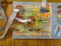
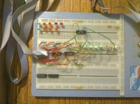
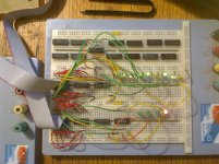
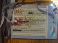
I have some Pictures that I can Now download, I couldn't do so earlier..

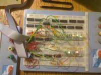
001.jpg 002.jpg


005.jpg 004.jpg

I have somethings to get done, I will Explain what they are later..

The Pictures are top left and right with 6000 entered on the Instruction Register..
The Pictures are bottom left and right with 6004 entered on the Instruction Register..
The top and bottom Left Pictures are of K19.. Pins 6 and 12, are the two Yellow Leds..
The top and bottom Right (Upper) Pictures are of M12, E3, and G13, with the Nine leds showing status to the right of the Ic's..
The top and bottom Right (Lower) Pictures are of K13, with the Four leds showing status to the right of the Ic's..


THANK YOU Marty
 
Last edited:
Ah - so the IR bits are really /IR bits (that was a bit of the puzzle I was missing).

If you invert the inputs to a gate you can't just change the gate from a NOR to an OR to compensate - you have to change it to a NAND or AND to get the same logic function (De Morgan's Theorem).

If the gates for combining /IR3-8 are now OR gates (and the inputs are all '1' when we have X00X in IR) then you have a problem - because an OR gate will have the same output whether it is being fed 11, 01 or 10. The output will only change state when we feed it 00.

Replacing K13 with a different logic gate will surely upset B4 on schematic LD12 and RAL on schematic LD16 won't it?

If you have replaced M12, E3 and G13 with OR gates, are the 'other' gates of these device(s) used elsewhere? If so, will that affect that logic also?

Dave
 
Hi All;

Thank You, Dave, for the update..

"" Ah - so the IR bits are really /IR bits (that was a bit of the puzzle I was missing). ""

Yes, I know..

"" If you invert the inputs to a gate you can't just change the gate from a NOR to an OR to compensate - you have to change it to a NAND or AND to get the same logic function (De Morgan's Theorem).

If the gates for combining /IR3-8 are now OR gates (and the inputs are all '1' when we have X00X in IR) then you have a problem - because an OR gate will have the same output whether it is being fed 11, 01 or 10. The output will only change state when we feed it 00. ""

Which is Part of my Solution.. In the BreadBoard, I tried a 7400, and ended up using a 7402, followed by the 7427..
And there are other things that I did..

When I get things back to working, I will send You a Picture of the Schematic, then it will make sense..

"" Replacing K13 with a different logic gate will surely upset B4 on schematic LD12 and RAL on schematic LD16 won't it? ""
"" If you have replaced M12, E3 and G13 with OR gates, are the 'other' gates of these device(s) used elsewhere? If so, will that affect that logic also? ""

Actually, it affected other things, Remember My gate assignments are not the same as Yours..
I Just use the Old Schematic for a common ground, so we are talking the same language..

But, In the end I only replaced the One Gate, not the whole IC..

Remember, that In the BreadBoard, I can make all kinds of changes, without affecting other Logic functions..

THANK YOU Marty
 
I await your schematic - which will hopefully make things clear as to your implementation. Although it may get a bit fuzzy the more egg nog I drink this Christmas Eve!

Dave
 
Hi All;

Dave, I quickly drew up the Schematic, before the Egg Nog takes effect..
For You to Evaluate, There are No Pin Numbers , nor Ic assignment numbers either..

006.jpg

I re-did what was on the BreadBoards, too much of a total mess before, And, I for some reason, am having trouble with the MA register, and I need to see if it was or is related to my changed schematic..
So I went to my old schematic using just the 7432 and the 7410, to see If the problem in the MA Register is still there, or not..
When I Run the Program..
NO, it shows the same problem, it's somewhere else..
Probably, a bent pin, stray wire or something like that..
I found a Stray wire buried in the mix.. Hopefully, that will help, taking it out that is..

THANK YOU Marty
 
Last edited:
I have had a quick look - and I can't see how this logic implementation should work (before the egg nog incidentally - just).

Take when /IR3=1 and /IR4=1. This would make the output from the top gate '0'.

If, however, we set /IR3=0 and /IR4=1 - the output is still a '0'.

If we set /IR3=1 and /IR4=0 - the output is still a '0'.

The output of the top gate would only ever go to a '1' when /IR3=0 and /IR4=0.

Since the whole action of this circuit is to decode when an IOT is performed on device 0 - I can't see how this can work as we require.

I assume IR7 and IR8 are active high and not active low on purpose?

I can't see why you would want /IR6 being used in one gate and its inverse in another.

The TOP gate (/IR3 and /IR4) should be an AND or NAND (as should the one with /IR4 and /IR6).

The gate with IR7 and IR8 should be an OR or NOR.

The three-input gate combining the signals would then depend upon what you went for for the two-input gates.

Dave
 
Hi All;

Dave, Thank You for Your Input, I wii need to take a closer look at what YOU are telling me in a Minute..

BUT, The whole Idea of this, is to do the following:

1. When it 'sees' a 6000 or a 6001, it will turn on or off the proper Gate..
BUT,
2. When it 'sees' a 604X it will NOT allow either of the Gates to to Turn ON..

3. When it 'sees' a 603X it will NOT allow either of the Gates to to Turn ON..

Now I know that I might need to put the '6' in along with the for-going logic, for a full decode, before it acts..

Hopefully, Now, (Maybe) that You hopefully understand what I am trying to do, I would gladly wire up any Schematic that will do what I am trying to do..

THANK YOU Marty
 
Back
Top