• Please review our updated Terms and Rules here

Cbm 2001 Pet strange boot

The scope will indicate a 'voltage' for UD2 pin 4 - what is it?
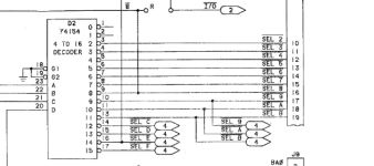
3,5V but i have only horizontal lines.....
"How" have you tried to detect pulses on UD2 pins 1 and 9? How have you setup the scope for this task?
Yes i set scope with all time/div but i can't see any pulses....i am desperate!!! Ud2 definitely fault????
So, have you an idea what that means ? We want to help you understand the process as well as fix this machine.
No...maybe bad Ud2???
 
Before we assume it is a bad UD2, put the NOP generator back in and recheck the UD2 output pins again. If you now get pulses, UD2 is not at fault.

Be especially suspicious of UD2 pin 4 and make sure that pin is Ok.

Dave
 
Before we assume it is a bad UD2, put the NOP generator back in and recheck the UD2 output pins again. If you now get pulses, UD2 is not at fault.

Be especially suspicious of UD2 pin 4 and make sure that pin is Ok.

Dave
Dave i am desperate now!! With NOP i have pulses on every ud2 output, also on pin 4!!!!!
 
What is the highest and lowest voltage on UD2 pin 4 then?

The pin can be not working correctly, but you still have a pulse on it! You stated previously that the voltage level was 3.5 Volts. This is still a logic '1' - but there is something wrong somewhere. However, UD2 could still pull the output down to logic '0'.

This is why you should always use your scope and look at the highest and lowest voltage and the leading and trailing edges for a nice, fast switch and minimum overshoot, undershorts and ringing.

Dave
 
I can see this in my new scope...in this analogic scope i can see only max level !
No, you can see both the upper and lower levels!
Set the switch from DC coupling to GND and adjust the Y position to ONE division ABOVE the base (as I told you to do many posts ago). Turn the switch back to DC coupling.
You can now see the upper and lower voltage levels (as you know where 0V/GND is).

Dave
Min: 0,2 V
Max: 3,6 V
 
So that pin does look suspicious. What is pin 4 actually connected to on the schematic before we warm up the soldering iron?!

Dave
 
If that is the only place it goes to (I can't open PDF files at the moment for some reason) then I would suggest changing UD2. Did your spare arrives?

Dave
 
If that is the only place it goes to (I can't open PDF files at the moment for some reason) then I would suggest changing UD2. Did your spare arrives?

Dave
Yes i received new UD2.
 

Attachments

  • Schermata 2022-06-17 alle 22.41.12.png
    Schermata 2022-06-17 alle 22.41.12.png
    45.9 KB · Views: 6
You do seem to be having a lot of problems with your machines!

Swapping UD2 should give you a working device but (since pin 4 is not (effectively) connected to anything), I don't think replacing it will actually solve your problem (unless there is another really strange internal IC fault).

Dave
 
You do seem to be having a lot of problems with your machines!

Swapping UD2 should give you a working device but (since pin 4 is not (effectively) connected to anything), I don't think replacing it will actually solve your problem (unless there is another really strange internal IC fault).

Dave
I am desperate!!!!! What can i do please???
 
So UD2

You have the NOP generator in ?

Pins 20,21,22 & 23 are showing waveforms ?

Do pins 8,9,10,11,12,13,14 & 15 show wave forms (these will be 5V with very short dips to 0V so you need to set your scope to trigger on a falling signal, then adjust the timebase until you can see it)
 
So UD2

You have the NOP generator in ?

Pins 20,21,22 & 23 are showing waveforms ?

Do pins 8,9,10,11,12,13,14 & 15 show wave forms (these will be 5V with very short dips to 0V so you need to set your scope to trigger on a falling signal, then adjust the timebase until you can see it)
Yes, with Nop inserted i can see waveform in every pin that you indicated to me, except for pin 12....in this pin i see only horizontal line :(
 
Look at the schematic and the data sheet for the device in question.

These are two basic things that you MUST learn to do.

If you do, you will find that pin 12 is not an output. In fact, you will not even see it identified at all on the schematic. If you look at the data sheet, you will see pin 12 is the GND power supply pin. Furthermore, you will notice the the VCC (+5 Volt) power supply pin is not identified on the schematic either!

Both of these are somewhat important pins!

Before I test pins of an IC, I generally test that there is a stable and healthy supply across the relevant pins. The 0V/GND pin is just as important as the VCC pin, so it is important to measure the supply actually on the two pins of the IC.

I had some IC’s on a PCB once that had the GND pin glitching to 1.3 Volts above the ground plane itself!

In general (but not always - check the data sheet) the GND and VCC pins are diametrically opposed pins of the IC. There are a few exceptions.

Could I suggest you start by looking at the data sheet for the 74LS00 and work your way up to more complex ICs on your PET?

Dave
 
I am desperate!!!!! What can i do please???

We can only follow where our test measurements lead us...

We find a fault, we fix the fault, we repeat this process until the machine works. It is as simple as that...

If the machine has 10 faulty chips, we have to find (and fix) the 10 faults before the machine will correctly work.

It is also possible that other things fail as we fault find. In this case, we have to go back to the beginning again and find the new fault...

Dave
 
Damn

Done it again ! read the wrong numbers on that stupid diagram :(

I meant pins 9,10,11,13,14,15,16,17

What I want to know is, do you understand how that chip functions ?
 
Back
Top