- VCF South West - June 14 - 16, Davidson-Gundy Alumni Center at University of Texas at Dallas
- VCF West - Aug 2 - 3, Computer History Museum, Mountain View, CA
- VCF Midwest - Sept 7 - 8 2024, Schaumburg, IL
- VCF SoCal - Mid February 2025, Location TBD, Southern CA
- VCF East - April 2025, Infoage Museum, Wall NJ
-
Please review our updated Terms and Rules here
You are using an out of date browser. It may not display this or other websites correctly.
You should upgrade or use an alternative browser.
You should upgrade or use an alternative browser.
Cbm pet 8296-d black screen
- Thread starter Desperado
- Start date
daver2
10k Member
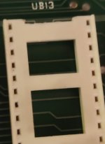
Ah. So eyes, a bright light and a magnifying glass to chase the PCB track from UB13 pin 7 to UC9 pin 5 to see where we are losing the signal at...
UB13 is sitting in its socket OK with pin 7 actually in the socket isn't it (rather than being curled up under the IC). Yes, I have had a fault like this before!
Dave
UB13 is sitting in its socket OK with pin 7 actually in the socket isn't it (rather than being curled up under the IC). Yes, I have had a fault like this before!
Dave
Desperado
Veteran Member
- Joined
- Nov 25, 2017
- Messages
- 6,827
YES because on ub13 pin7 i have pulsing signal if i touch pin with probe..i don't have continuity between ub13 pin7 and uc9 pin 5UB13 is sitting in its socket OK with pin 7 actually in the socket isn't it (rather than being curled up under the IC). Yes, I have had a fault like this before!

daver2
10k Member
Possibly?
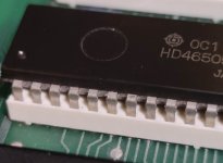
Can you post a close up photograph of that pin?
It will certainly mess up the display we see - by displaying some of the wrong characters. Not sure why my PETTESTER didn't move on - but this could be masking another fault with the video sub-system of course.
Dave
Can you post a close up photograph of that pin?
It will certainly mess up the display we see - by displaying some of the wrong characters. Not sure why my PETTESTER didn't move on - but this could be masking another fault with the video sub-system of course.
Dave
daver2
10k Member
Excellent. I know it may sound a bit bizarre - but this is better!
I need to check the characters in more detail later just to make sure - but it looks like things are being written and displayed properly now.
I just need to work out in my own mind why that particular fault caused the video display that we originally saw.
If the characters are displayed correctly - but the PETTESTER is not 'moving on' in its tests - this indicates that the firmware is not reading back correctly what it wrote - therefore, some of the READ buffers in the 74LS244's are not working as they should.
That's my assessment any how.
I think that is good work for today though. I believe some 'subdued' celebrations are caused for to get this far!!!
Dave
daver2
10k Member
So, TA3 from the CRTC is multiplexed with buffered address line 4 (BA4).
When the video sub-system performs a read (based upon address signals from the CRTC) it does so a WORD at a time, latching the results into the ODD latch (UB8) and the EVEN latch (UB3). The video sub-system takes the bits first from the EVEN latch and then from the ODD latch before requesting data from the next WORD and so forth.
The CPU (on the other hand) is an 8-bit device, so handles the video RAM in units of bytes. Buffered address 0 (BA0) selects between the EVEN video RAM (BA0=0) or the ODD video RAM (BA0=1).
TA3 is multiplexed with BA4 - hence (from the CPUs perspective) it is writing to byte 16 (decimal) = 1000 (binary) whereas the CRTC and video sub-system is performing word reads on address 8 (decimal) = 100 (binary).
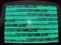
With TA3 being stuck HIGH - it meant that the 8 lower words (where TA3 should have been LOW) being misread from the 8 upper words (where TA3 is HIGH). The next block of reads (where TA3 should have been HIGH) would have been (correctly) read from the right place in video memory.
This means that the upper 8 WORDS (16 BYTES) containing the characters 'p q r s t ...' were duplicated where '@ a b c d e ...' should have been - and this is what we observed.
We (well me) were 'fixated' on data bit 4 - but it was address bit 4 (TA3) that was at fault.
OK, so I will double-check the displayed characters after tea and then think about how to debug the read buffers later.
Dave
When the video sub-system performs a read (based upon address signals from the CRTC) it does so a WORD at a time, latching the results into the ODD latch (UB8) and the EVEN latch (UB3). The video sub-system takes the bits first from the EVEN latch and then from the ODD latch before requesting data from the next WORD and so forth.
The CPU (on the other hand) is an 8-bit device, so handles the video RAM in units of bytes. Buffered address 0 (BA0) selects between the EVEN video RAM (BA0=0) or the ODD video RAM (BA0=1).
TA3 is multiplexed with BA4 - hence (from the CPUs perspective) it is writing to byte 16 (decimal) = 1000 (binary) whereas the CRTC and video sub-system is performing word reads on address 8 (decimal) = 100 (binary).
With TA3 being stuck HIGH - it meant that the 8 lower words (where TA3 should have been LOW) being misread from the 8 upper words (where TA3 is HIGH). The next block of reads (where TA3 should have been HIGH) would have been (correctly) read from the right place in video memory.
This means that the upper 8 WORDS (16 BYTES) containing the characters 'p q r s t ...' were duplicated where '@ a b c d e ...' should have been - and this is what we observed.
We (well me) were 'fixated' on data bit 4 - but it was address bit 4 (TA3) that was at fault.
OK, so I will double-check the displayed characters after tea and then think about how to debug the read buffers later.
Dave
daver2
10k Member
>>> Yes! Great job! Possible that i have other bad contact between pin and sockets?
Well, you can bus them all out with your multimeter. Although I don't think the problem is the CRTC anymore - but the LS244 buffers.
Dave
Well, you can bus them all out with your multimeter. Although I don't think the problem is the CRTC anymore - but the LS244 buffers.
Dave
daver2
10k Member
Yes, you will - good thinking for performing the test though...
If you go back to post #291 and look at the documentation I wrote for the PETTESTER firmware (on page 3 of 16) you will observe what a 'good' 80 column display should look like. You can print this page out and check your PET screen yourself.
Before we move forwards tomorrow - I think we should repeat some of the measurements again (with the logic probe) to ensure that things that appeared to work before are still working now.
Dave
Desperado
Veteran Member
- Joined
- Nov 25, 2017
- Messages
- 6,827
Just checked, it's the same finally !!!If you go back to post #291 and look at the documentation I wrote for the PETTESTER firmware (on page 3 of 16) you will observe what a 'good' 80 column display should look like. You can print this page out and check your PET screen yourself.
daver2
10k Member
Excellent!
Right, so I need to give you some continuity checks to do with the power off using your multimeter.
First of all print out this schematic http://www.zimmers.net/anonftp/pub/cbm/schematics/computers/pet/8032/8032029-09.gif.
Next, look at the signals named OSD0, OSD1, ..., OSD7.
They go from the RAM (UC6 and UC7) to the 8-bit latch (UB8) and to the buffers (UB6 and UB7).
Work from OSD0 through to OSD7.
With one probe of your multimeter on OSD0 on the associated RAM chip (in this case UC6 pin 14) test for continuity to all of the other locations it is supposed to go to with the other probe of your multimeter (i.e. UB8 pin 3, UB6 pin 2 and UB6 pin 3).
Move on to the next OSDx signal and repeat for them all.
After that, repeat the same process with the signals ESDx found on schematic http://www.zimmers.net/anonftp/pub/cbm/schematics/computers/pet/8032/8032029-08.gif.
We have to do the same with another schematic - but I will give you that homework after you have done this!
Obviously, check with your multimeter probes on the pins of each IC to ensure full continuity.
What we are ensuring is that pins that should be wired together actually are!
Dave
Right, so I need to give you some continuity checks to do with the power off using your multimeter.
First of all print out this schematic http://www.zimmers.net/anonftp/pub/cbm/schematics/computers/pet/8032/8032029-09.gif.
Next, look at the signals named OSD0, OSD1, ..., OSD7.
They go from the RAM (UC6 and UC7) to the 8-bit latch (UB8) and to the buffers (UB6 and UB7).
Work from OSD0 through to OSD7.
With one probe of your multimeter on OSD0 on the associated RAM chip (in this case UC6 pin 14) test for continuity to all of the other locations it is supposed to go to with the other probe of your multimeter (i.e. UB8 pin 3, UB6 pin 2 and UB6 pin 3).
Move on to the next OSDx signal and repeat for them all.
After that, repeat the same process with the signals ESDx found on schematic http://www.zimmers.net/anonftp/pub/cbm/schematics/computers/pet/8032/8032029-08.gif.
We have to do the same with another schematic - but I will give you that homework after you have done this
!Obviously, check with your multimeter probes on the pins of each IC to ensure full continuity.
What we are ensuring is that pins that should be wired together actually are!
Dave
Desperado
Veteran Member
- Joined
- Nov 25, 2017
- Messages
- 6,827
Well!Excellent!
Right, so I need to give you some continuity checks to do with the power off using your multimeter.
First of all print out this schematic http://www.zimmers.net/anonftp/pub/cbm/schematics/computers/pet/8032/8032029-09.gif.
Next, look at the signals named OSD0, OSD1, ..., OSD7.
They go from the RAM (UC6 and UC7) to the 8-bit latch (UB8) and to the buffers (UB6 and UB7).
Work from OSD0 through to OSD7.
With one probe of your multimeter on OSD0 on the associated RAM chip (in this case UC6 pin 14) test for continuity to all of the other locations it is supposed to go to with the other probe of your multimeter (i.e. UB8 pin 3, UB6 pin 2 and UB6 pin 3).
Move on to the next OSDx signal and repeat for them all.
After that, repeat the same process with the signals ESDx found on schematic http://www.zimmers.net/anonftp/pub/cbm/schematics/computers/pet/8032/8032029-08.gif.
We have to do the same with another schematic - but I will give you that homework after you have done this
Obviously, check with your multimeter probes on the pins of each IC to ensure full continuity.
What we are ensuring is that pins that should be wired together actually are!
Dave
Ok i print these pages and i prepare my multimeter....
Thanks so much! Have a good dinner !
daver2
10k Member
Excellent!
You now need to repeat the continuity tests with the signals called BD0 to BD7. For this you will need a new schematic (http://www.zimmers.net/anonftp/pub/cbm/schematics/computers/pet/8032/8032029-01.gif) in addition to the two schematics you already have.
Let’s start with BD0 shall we?
Put one of your multimeter probes on UB10 pin 17, and then chase this signal around the other places it goes:
UB10 pin 18.
Then over to schematics 8 and 9 (that you already have) with UB4 pins 17 and 18 and UB6 pins 17 and 18.
Repeat for signals BD1 through BD7.
Dave
Desperado
Veteran Member
- Joined
- Nov 25, 2017
- Messages
- 6,827
Good Sunday Dave,Excellent!
You now need to repeat the continuity tests with the signals called BD0 to BD7. For this you will need a new schematic (http://www.zimmers.net/anonftp/pub/cbm/schematics/computers/pet/8032/8032029-01.gif) in addition to the two schematics you already have.
Let’s start with BD0 shall we?
Put one of your multimeter probes on UB10 pin 17, and then chase this signal around the other places it goes:
UB10 pin 18.
Then over to schematics 8 and 9 (that you already have) with UB4 pins 17 and 18 and UB6 pins 17 and 18.
Repeat for signals BD1 through BD7.
Dave
this job is done! Continuity test ok!!