• Please review our updated Terms and Rules here

Commodore 1801 crooked picture and convergence(?) issues

PS: ...there is enough overshoot in that signal waveform that a VDU working normally with a good flat frequency response in the video amplifiers at least to the 5 to 7MHz region, would faithfully reproduce those overshoots and therefore you could expect to see it in the screen image. If there was even a little HF peaking on top of that, in the VDU's video stages/amplifiers, it would enhance the effect.
Some VDU's were built with a control called "Aperture" so the user could adjust the HF response to their liking.

(On the topic of the 2465B and my love affair with them, I like mine so much it is hard to go to any other scope. Although rated for 400MHz bandwidth, their vertical amplifiers and trigger circuits are still able to lock and display a 900MHz wave. They were built with a large number of Tek designed ASIC's, though they are under some digital controls from the CPU board, but the signal pathway is Analog and they have excellent cursor measurement functions. And the CRT is a total mind blowing masterpiece of Electron Optics that the World will never see again and they are readily repairable with an excellent service manual. I invested in all the Tek calibration generators for mine as I refuse to send them out to external calibration services).
 
Last edited:
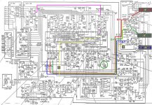
I have drawn over the schematic. It is less likely the R-Y, B-Y and G-Y signals would have the frequency response defect equally but worth checking. In this design the video output transistor inverts those signals because it is cathode drive to the CRT, not grid drive. Also the matrixing is done by mixing -Y (the luminance signal with the possible frequency response defect) into the video output transistor's emitters, so it appears at their collectors to cancel the the +Y there. So you end up with -R, -B and -G at the CRT's cathodes.

As you can see the composite signal passes through a delay and some frequency response altering components into pin 27 of the IC.

Once the signal feeding the VDU is verified to be free from overshoot errors, the first place to scope is pin 27. The TONE pot, alters the frequency response too and ultimately the clamped luminance signal (devoid of any chroma) comes out of pin 5 of the IC, the next place to scope.

Then you could scope around the video output transistors base & collector circuits. The capacitors across the emitter resistors of the video output transistors, boost the HF response. If you find for example the signals at the bases look ok and there is overshoot at the collectors, those values can be reduced or a resistor placed in series with each capacitor to limit the HF boost.
 

Attachments

  • VDU.jpg
    VDU.jpg
    511.8 KB · Views: 5
Excellent quality scope recording, that is the sort of thing I am used to. It does have a blacker than black overshoot which I did not draw on the diagram I posted as I was not sure if it was there.

When you connected the C64 signal directly to the scope, did you terminate it at the scope end with a 75R BNC terminating resistor (on an inline plug or a BNC type on a T fitting) with the scope input on high Z, or was the scope set to high Z on its own in or 50R input mode ?
Exactly, it's a T-piece with a 75R BNC termination without using 50R termination of the scope. No idea about the other modes in the context of video signals... High-Z? Do you mean the regular 1MOhm inputs?

Lets say the source signal still looks like that , connect into a 75R load, then it could be a combination of factors, in that the source signal may contain the overshoots, but the other VDU's you have tried don't display it because they have a lower overall HF response in the video circuits have rolled it off.
I was able to see the slight peak on my 1084, but only with composite video and when turning up brightness and contrast.
I will have a look at the schematic and work out the places along the way to test the signal in your VDU.

"Which pattern do you recommend for fault finding?"

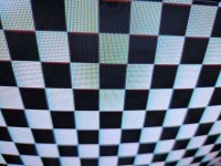
Well for this particular issue the checkerboard because it shows up the overshoot issue well on a black to peak white and white to black transition. For other issues like scan linearity or doing convergence adjustments it is best to use the crosshatch pattern, but for convergence the Dot pattern works well too, and for other issues the greyscale and or color bars depending what the problem is.
Unfortunately no dot pattern, but I guess the crosshatch will do.
PS: ...there is enough overshoot in that signal waveform that a VDU working normally with a good flat frequency response in the video amplifiers at least to the 5 to 7MHz region, would faithfully reproduce those overshoots and therefore you could expect to see it in the screen image. If there was even a little HF peaking on top of that, in the VDU's video stages/amplifiers, it would enhance the effect.
Some VDU's were built with a control called "Aperture" so the user could adjust the HF response to their liking.
I was thinking there might be an adjustment for that, apparently it's not that easy on this monitor.
(On the topic of the 2465B and my love affair with them, I like mine so much it is hard to go to any other scope. Although rated for 400MHz bandwidth, their vertical amplifiers and trigger circuits are still able to lock and display a 900MHz wave. They were built with a large number of Tek designed ASIC's, though they are under some digital controls from the CPU board, but the signal pathway is Analog and they have excellent cursor measurement functions. And the CRT is a total mind blowing masterpiece of Electron Optics that the World will never see again and they are readily repairable with an excellent service manual. I invested in all the Tek calibration generators for mine as I refuse to send them out to external calibration services).
It does really have superior triggering compared to my DS1054z. I immediately jumped on the next best opportunity to get a good one! It is more satisfying to use than the DSO... I hope I don't have to calibrate soon because I lack any of that gear and knowledge...
I have drawn over the schematic. It is less likely the R-Y, B-Y and G-Y signals would have the frequency response defect equally but worth checking. In this design the video output transistor inverts those signals because it is cathode drive to the CRT, not grid drive. Also the matrixing is done by mixing -Y (the luminance signal with the possible frequency response defect) into the video output transistor's emitters, so it appears at their collectors to cancel the the +Y there. So you end up with -R, -B and -G at the CRT's cathodes.
Wow, you really are some kind of CRT wizard :) thanks for identifying the relevant circuits!
As you can see the composite signal passes through a delay and some frequency response altering components into pin 27 of the IC.

Once the signal feeding the VDU is verified to be free from overshoot errors, the first place to scope is pin 27. The TONE pot, alters the frequency response too and ultimately the clamped luminance signal (devoid of any chroma) comes out of pin 5 of the IC, the next place to scope.
The TONE control changes it, but ultimately doesn't seem to solve it.. there's still some overshoot even when turned all the way to "smooth", at which point it looks washed out...
Pin 27 has very slight overshoot, but nothing that would suggest this picture. At pin 5, the signal looks OK, but I'm not really sure because it was difficult to get a proper measurement due to the interference from the HV. I'll try to find a better spot to measure.
Then you could scope around the video output transistors base & collector circuits. The capacitors across the emitter resistors of the video output transistors, boost the HF response. If you find for example the signals at the bases look ok and there is overshoot at the collectors, those values can be reduced or a resistor placed in series with each capacitor to limit the HF boost.
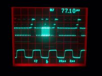
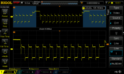
At the base I could not find a useful signal, but the collector show the peaks very clearly:
1801-q701-collector.png
I wasn't able to take proper pictures from the Tek during daylight because of the glare on the screen, but I'll do so in the evening when I can darken the room properly. I'll report back when I have more insight about the Luma signal.
 
If the B-Y, R-Y and G-Y signals out of the IC pins 1,2 & 3 look ok and the -Y signal looks ok too on pin 5 and the overshoots are largely at the collectors of the three video output transistors, they are likely being caused by the emitter resistor bypass capacitors, the two 560pF capacitors and the 390pF capacitor. Often the high frequency response will be inadequate without them, and some capacitance is required to sharpen up the image edges, but the values might be excessive over-doing the HF boost. The pF values might need to be 1/3 to half what they are.

The thing to do is to just disconnect one leg of each of the three capacitors (all three for the test) with solder wick works well if its a single sided pcb and see what happens to the problem. However the output stage/s might be compensated to a flat frequency response and just be amplifying the waves they are fed with containing the overshoots. Still even with that, the effect could then be knocked back by lowering the three capacitor values.

The ideal values will come down to what you see on the screen itself, because, even with the x10 probe, its about 10pF input capacitance will slightly affect the frequency response when it is connected.

(yes, high Z meaning the regular 1M Ohm input)
 
Last edited:
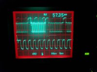
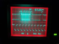
I still can't make out anything on pins 1-3.. looks like noise to me. Anyway, it seems like you were right, this is how it looks like:

-Y signal:

1801-luminance.jpg

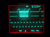
Collector before desoldering capacitors:

1801-output-before.jpg

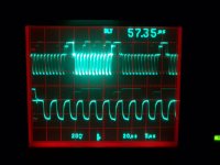
After:


1801-output-after.jpg

If I turn the TONE to maximum sharpness it's almost good now. Wow, good job! :)

I'm going to be away from the monitor for a few days, but at this stage I'll have to source capacitors anyway.. can't wait to try it!
 
Try initially changing the two 560pF caps to 220pF and the 390pF to 180pF. You might need to go lower in value.

It is an interesting task to correctly frequency compensate the common emitter amplifier with bypass caps (or frequency selective networks) across its emitter resistor.

You will find that as you make the capacitor smaller, the overshoot will get narrower and of lower amplitude, until the amplitude of the peak is about equal to, or a tad higher than the flat top of the square wave (somewhat similar to adjusting the compensation capacitor on a scope probe with a square wave test) the idea being to get the amplified square wave to have the best rectangular corner possible.

Sometimes, when that bypass cap is just right, to get a square edge on the wave without significant overshoots, there can be a small dip in the flat top of the wave immediately after the corner. If it is significant that is normally remedied with a series resistor and larger value capacitor placed across the emitter resistor too and the resistor made adjustable. This boosts a lower frequency than the fast rise. (the square wave can be thought of as being composed of sine wave with multiple higher 3rd order harmonic frequencies, so the flat top of the square wave is composed of the lower order harmonics than the fast rise).

In oscilloscope vertical amplifier design, the same problem remains, because you want to have the vertical amplifiers, right up to the CRT's deflection pates have perfect fidelity and a perfect square wave response.

Tek were total masters at this and provided multiple adjustments here to get the square wave response perfect. A while back I wrote an article explaining how this works for the Tek 464/466 scopes and the principles are just the same for the single ended amplifier, like the video output transistors in a VDU, as they are for paraphase (push pull) amplifiers in a scope's vertical amplifier system. The commonly used frequency compensating networks in scopes are on pages 6 & 7:

 
Hello, I'm back from holidays and have received the capacitors.

Very interesting article, but I admit I barely understood about 1/3 of it... I can imagine where I need to go with these modifications though.

I have temporarily changed the capacitors with the suggested values (just tacked them on without clipping the legs), this is the result with the trimpot all the way down (left) and in its mechanical center position (right picture)
1801-9.jpg1801-10.jpg

Subjectively, it looks already better... but it's stil not too square. Do I need the larger value capacitor and/or series resistor?

1801-11.jpg

It's already acceptable for me, but if you have a suggestion on how to improve it further I could give it a try
 
You could increase the capacitor values now a little, it will take some experimenting. The ideal value will be when the signal looks a little squarer on the scope, but without the scope connected you should not see any overshoot on the screen image on the leading edges (left had side of the white blocks). The effect of the scope probe's capacitance means that it will result in the waveform looking a tad more rounded off than it actually is, when the probe is not connected. It is possible that they deliberately peaked the response a little to help see text & graphics, so check with some white text too if you have a signal.
It does not look like any series resistors will be required.
 
Ok, after playing around with some values it didn't really get better and I decided to put it aside for the moment to continue on other projects. I've permanently replaced the capacitors with the values suggested initially (2x 220pf and 1x 180pf) and tried to adjust the crookendness and convergence, which turned out way more fiddly and aggravating than I thought.

In the end, it slightly improved the picture but it's not perfect yet. During normal use it's not bothersome anymore and I'll be revisting it at some point the future when I run out of things to do.

Another reason to put this on hold is that my Tektronix 2465B is starting to act up and I need to have a look at it before the PSU blows up and smokes up my room.

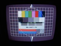
Picture of the 'result':
1801-12.jpg

Thanks a lot for your help, it was really interesting following the signals and I think I've learned something about CRTs and analog video circuitry.
 
Last edited:
Back
Top