Gary C
Veteran Member
I am going to update the kicad with that change.
HOWEVER, I would not 'short it out' until a few other people have had a look and voiced their opinions. Shorting something to the +5V rail is quite drastic. Myself, I would probably pull it to +5V using a 1k resistor.
Yep just checked the board, IC62 pin 1 has a small trace to up to the GND rail (as does 3 & 8).Can you also check IC62 pins 1 and 16 please. Both of these should be connected (via a similar bit of 'magic copper') to 0V. If this is not there - this could well be messing up our DMA address (again, not that it will make any difference to your problem in the short term, but it will in the longer term). It could also indicate a more wide-spread issue that we may need to address...
Ok so back to this test and now that I'm looking at the correct (output) channels:After that, we will be looking at the A, B, C and D outputs from ICs 32 and 33.
When the /L pin is LOW, the outputs should be preset to ABCD = 1000.
When the /L pin is HIGH, IC 32 and 33 should count up from the initial value of 1000. The carry from IC 33 should count +1 into IC 32.
>>> D5 = 1/0 doesn't seem to impact any of these pins.
Correct.
IC32 and IC33 are the fundamental counters for the state machine.
Did you see the bit about triggering the oscilloscope on /L and working your way forward through the logic?
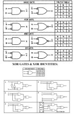
Check the inputs to the simple gates and work out what the output should be (from the AND or OR truth table) and see if that is what you get on the output of the gate you are checking.
At some point, we must find some missing pulses that should be there...
Dave
Yep.I did see this but am not very clear on the test procedure. These gates you're referring to are IC's 8, 20, 21, 22 and 30 - correct? Guess it's time I learned how to read/interpret these truth tables anyways! :D I'll see what I can do.
This is why it is important to enter the schematics as well as the PCB layout. The Design Rules Checker (DRC) can then test for stupidities - i.e. PCB tracks where there are none on the schematic and missing PCB tracks where they should be present. In order for a fault to 'sneak through' you would have to make an identical mistake on both the schematic and the PCB layout.
Dave
Currently my Sol is in a storage location to make space for other antics on my bench and the Dazzler boards not fitted.It would probably help if @Hugo Holden could probe IC8 pin 6 for us with his oscilloscope and post what he is observing.
Perhaps by setting Dazzler port 0Eh to 80h and port 0Fh to 59h (x4 resolution, 512B memory, colour, high brightness RED) and then 19h (x1 resolution, 512B memory, colour).
After you have sorted out the poodles, I have worked out how the colour DAC works, so we can do a few simple checks with the oscilloscope for a bit of light relief from the system controller logic.
Dave