• Please review our updated Terms and Rules here

Debugging a KIM-1 computer

Hi Dave
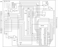
It is funny that I'd originally bought a 74138 with intentions
of using that. When I started the drawing I couldn't recall why I'd
bought it.
I still need an inverter for the R/W on the EEPROM or I'll not be able
to do in place programming. I'd really like to keep that.
I just realized that K6/7 is OK for reading but needs CLK2 for writes.
I have some cleanup to do.
Dwight
 
Last edited:
With the 74138 you can do some quite elaborate decoding, it has three direct 'address bits' and two active low and one active high level 'enable' line, all 8 outputs are active low (for /OE, /CS, /RD or /WR etc)..
 
I'll have to reevaluate what I'll do for decoding there. It may be two chips or
a 16L4 type device.

I really hope you can keep your elegant design concept of stacking everything using only the 6532 40 pin footprint.

The GAL16V8 can be obtained in small outline (SOIC) and PLCC packages if needed to make everything fit. I would have to build some surface mount-to-DIP adapter in order to program them. It is more than enough to do all the address decoder/glue logic in one part. Looking at ebay, the PLCC is the most common surface mount package and can be bought for less than a buck in very small quantities.

A real drawback is that the kit would have to come with a programmed GAL as it can't be expected that all the users would have the capability to program PAL/GALs.
 
I'm going to go with one 7404 and one 7400. I should still be able to keep
it small.
It looks like a minimal gating takes 5 inverters and 3 nands. That includes
the gating needed for the EEPROMs WE*.
I'll update the drawings tomorrow.
The SOIC ttl parts are really small.
I looked at using the 74138 but it didn't solve the EEPROM write problem.
It needs either the WE* or the CE* qualified with CLK2. It doesn't make
sense to add it to CE* because one wants to not have it for the read.
It is needed for the write though.
I looked at the 6502 timing and there should be no issue programming the
EEPROM. I'll probably write code for the D7 compliment write testing.
I'm really pissed at myself for messing up the decoding.
That is why one does a prototype of every thing.
Dwight
 
I'm going to go with one 7404 and one 7400. I should still be able to keep
it small.

Dwight,
Good work. If you can keep the footprint without the need for a PAL/GAL, so much the better.

I looked on ebay for a KIM-1. Working units are very expensive, while a broken one may have a bad 6530. Your repair kit will be a viable option.
-Dave
 
I redid the schematic but forgot to hit the send button. It'll have to wait for
tomorrow.
Dwight

Got it now.
Dave, you have a good eye, can you review it?
I have a few redundant wires shown that are in the first drawing.
If I get time, I'll delete them in the first drawing to remove confusion.
Thanks
Dwight
 

Attachments

  • adapt1.jpg
    adapt1.jpg
    90.6 KB · Views: 6
Last edited:
can you review it?

Dwight,
Looks good. I think you got it. I was a little confused until I realized CS1 on your schematic is the K5 decoder output on the KIM-1. You may want to denote that on the schematic.

To make the 6530 replacement kit a universal design, I think you need add jumper selects into the 6532 CS1, /CS2 and /RS inputs to open the circuits and allow jumpers to any address line that may be required. But more than that I notice that the 6530 in the 4040 disk drive uses pin 19 as a chip enable while the KIM-1 uses pin 18. So cut and jumpers may be needed for some applications anyway.
-Dave
 
I thought about that but I wanted to keep it simple for the KIM-1 only.
Others have made adapters for Commodore stuff. They weren't as clean
as this one will be.
I've decided to use a PLCC 16L8 instead of the separate gates. It'll add a little
bit of height but a lot simpler wiring for the PC. You just bring the wire to
whatever input you'd like to use. The only restricted areas are the outputs.
One can skip every other pin ( cut them off once programmed ) to use for
more routing. Routing is going to be the bigger issue.
Also, I wanted to make it so one could change it form -002 to -003 for both
the I/O and the ROM. The way it is now it would take another chip to be able to do that.
One still has to program both ROM sections but that will be easy with the debug
board. The 16L8 is so much more flexible and actually uses less board space.
I just wish it were flatter. I can bring more wires to the 16L8 to make it more
universal. It could have all the signals use in the original 6530!
I've settled on using KiCad. Both cheap and many think it is quite good.
CS1 is the proper name of the 6530 pin, when used as a select.
Dwight
 
The prototype adapter is working, at least for the first level. My display test works.
Now for my next trick to see if I can write to the EEPROM.
I may still have other issues but it is a lot easier to check things with a
working monitor. I will continue to write more EPROM drive test. It is just that
things are so much easier if I know all is working.
I'd bought some cheap 6532s from China. The first one was dead so I suspect
something else may be bad in the part that is working so far, maybe RAM or timer.
I was worried the there was something wrong with the adapter ( some 50 or so
crossed wires ).
Still, a working KIM monitor will make the job a little easier than not knowing if
there was a problem in my code or in the hardware.
Dwight
 
Thanks for the pointer.

I was looking on the adapter and the data sheet for the EEPROM.
I have G* and E* swapped. I'll fix that before running my code to program
the -002 data.
I'll post a new schematic soon. I want to make sure there are no other issues.
Dwight
 
I'm having problems programming the EEPROM. I've read the spec
several times and think I got it right.
I'd got the EEPROM from Anchor Electronics and I suspect it has the
software protect enabled. I may have miswired something as well.
I'd not setup the addressing to be able to undo the software disable
so I had to rip it out to rewire. I had it nicely tucked under the sockets
but now it'll dangle off to the side because I'm not digging in there again.
Anyway I'll want it off to the side where I can put an oscilloscope on
it.
I'd just put pullups on the unused addresses. I'm going to need to attach
the odd and even address, A10, A11 and A12, to odd and even addresses
that are being use. In other words, connect A12 to A8, A11 to A9 and A10
to A6 as pairs. That way I can do 1555 and 0AAA addresses needed.
I suspect that Anchor got some NOS that had been preprogrammed and software
locked. I can use the software lock rather than a jumper on the WE\ pin.
I only need the jumper for -002 and -003, making things simpler.
Dwight
 
Last edited:
I'd got the EEPROM from Anchor Electronics and I suspect it has the
software protect enabled.

What brand of 28C64? SEEQ, Xicor, NEC, ? They should be erasable in your PROM Programmer no matter any software protect. I think the most Programmers erase the part before programming new data.

Most 28C64's allow +12V on the OE signal (pin 22) with CE and WE low for 10mS to erase the chip.
 
It is a ST M28C64A. The data sheet seem to indicate that
the A type doesn't support the bulk erase.
I'd swapped the WR* and G* wires so it wasn't right.
I've swapped the wires but still have no luck. I've not yet
tried the soft protect disable.
I'll do that this morning.
Dwight
 
Success!!!
Between bungling the code, the programmer and the swapped
wire, I'd had a lot of mistakes.
I've booted the KIM to the EEPROM. Yaaaaeeee!
Now to learn to do the KIM input.
Also write some more test code.
Part of the problem was that after fixing the swapped wire,
I'd been using the EPROM programmer wrong. It has a separate
step to enter the file name and then transfer the file to
its buffer. I'd been to frazzled that I realized that I didn't
remember to transfer the file to the buffer ( separate step ).
There was so many steps and I was just wearing down.
I have the LED doing two things. If the code is loading, it
flashes fast and then goes out if it worked.
If it failed it would come on steady. I've been seeing the
steady light so much I'd just about given up.

Early on, I realized that once I switched the ROM to be the -002
image, I'd lose the NMI vector in my boot image. The KIM expects
it to vector through the RAM at $17FA. I've not written the test
code yet to check the RAM in the -002 or the -003 so I'd modified
my -002 image to go to my EEPROM programming code in RAM.
I need to test that RAM to make sure it will take the
jump to interrupt vector. Then I can have a clean image.
I'd done that to minimize the variables.
I'll write code to patch the correct vector in the EEPROM as
part of the programming code.
It is all complicated.
Dwight
 
Sorry for the long delay on getting back on progress.
I've made a prototype run of boards. I've not checked the adapter boards
yet because I'm waiting on a friend that is blowing the PAL fuses for
me.
The debug has a couple non-functional issues but otherwise works.
I did forgot the pullup resistors on the K3, K4 and DEN lines. I'll fix this on then
main run of boards. For now, I'll tack on resistors.
I'd not made the solder mask clearance on the bottom of the board
for the connectors ( required some scrapping ).
The adapter boards ( 2 are stacked ) had the holes for the interconnect
too small. I'd planned on using 28 ga. wire but the holes only fit 30 ga.
I'm glad I'd made a proto run.
Considering that this is my first boards I'm reasonably happy.
I've got a connector issue. The 44 pin connectors I located don't have
enough end clearance, for more blank board at the ends of the pins. I'm thinking
I may just use a small end mill the extend the ends.
Dwight
 
pictures:
One shows the two small adapter boards that would go under the
6532, to replace the 6530.
The other shows the debug board attached to the extension connector.
Notice the rats nest in place of the 6530-002. To the right of the 6532 is
the EEPROM holding the -002 code. The other dark blob is the two logic
chips that form the address decoding.
The first two small boards replace these.
I'll have an update this weekend with the small boards put together
and hopefully working.
Dwight
 

Attachments

  • IMG_4683.jpg
    IMG_4683.jpg
    91.6 KB · Views: 11
  • IMG_4682.jpg
    IMG_4682.jpg
    94.2 KB · Views: 11
I finally got around to debugging my adapter. It is often hard to debug ones own work. Especially when you get older. I had everything working except for the phase of clk2. Luckily it is a PAL change so it is a simple source change. I chose the wrong phase for what the board had.
I was going to post a picture but I can't figure how to do that on this new MB. I can't even see my older pictures?
I'll make a run of the corrected boards.
The adapter had 2 issues. The board interconnect holes were two small ( I had to use 30 ga. wire instead of the planned 28 ga. ). I also missed one wire.
The debug board missed a three pullup resistors but otherwise worked fine.
My progress has been slow but I'm finally seeing the end.
I've written most all of the debug code for the debug board. I need to write up the instructions as well.
Progress is being made.
Dwight

IMG_4691.jpg

You can see the wire to U16 for the proper clock. It will be fixed in the next PAL.
 
Last edited:
Back
Top