• Please review our updated Terms and Rules here

Heathkit H89A Question

Yes,

Most of the pins look sensible - but with a couple of exceptions. Please check the following pins out on the Z80 CPU with your oscilloscope to see whether there is any activity on them or not. Your pins 19 and 20 being 0V is a concern also!

Pin 19 /MREQ.
Pin 20 /IORQ.
Pin 21 /RD.
Pin 22 /WR.
Pin 27 /M1.
Pin 28 /RFSH.

I would expect activity on ALL of these pins if the Z80 is working correctly.

I suspect pin 16 (/INT) is permanently LOW because the Z80 is not processing the interrupt correctly.

ROMs contain code (in general) so they are not interchangeable (unless they contain the same code of course). I assume, therefore, that you do not have an EPROM programmer?

No problem to giving you help. It doesn't take much of my time, and you are doing the hard bit!

Dave
 
Last edited:
I will write you a little explanation of how the Z80 works (OK, very simplified) tomorrow when I have a real keyboard to type on and not my phone.

Hopefully, this will give you the knowledge to understand what the above control signals do and how they are manipulated to access memory and I/O ports.

Dave
 
The Z80 is an 8-bit microprocessor.

The address bus contains 16 address lines (identified as A0 to A15) and this bus is used by the Z80 to select one of 64KB (65,536) memory locations (each of 8 bits). 1KB = 1,024 Bytes in computer parlance. 2^16 (where 16 is the number of address lines) = 65,536 = 65,536/1,024 = 64K. A lower case 'k' (as applied by units) stands for x1000 whereas an upper case 'K' stands for x1,024.

The Z80 outputs the desired address on the address bus to select the desired memory location to read or write.

The Z80 (being an 8-bit CPU) has an 8-bit data bus (identified as D0 to D7). The data bus is used to transfer a byte of data from the CPU to the memory (on a WRITE cycle) or a byte of data from the memory to the CPU (on a READ cycle). The memory location is specified by the CPU on the address bus.

This leaves all of the other signals - collectively known as the control bus.

Some CPUs (e.g. the Motorola 680X and 680XX) use memory locations to address peripheral (I/O) devices (e.g. serial ports). Unlike these CPUs, the Z80 can (and usually does) address peripheral devices separately to memory. This is known as I/O space. There are 256 bytes of I/O space - addressed by the CPU on A0 to A7.

So, how does the memory and peripheral devices 'know' what to do when the Z80 puts an address on the address bus? The answer is the signals on the control bus:

/RD tells the memory or I/O devices that the Z80 CPU wishes to read something. The data from the addressed memory or peripheral device should be placed onto the data bus for the Z80 CPU.

/WR tells the memory or I/O devices that the Z80 CPU wishes to write something. The data to the addressed memory or peripheral device has already been placed on the data bus by the Z80 CPU.

/MREQ tells the external address decoding logic that the Z80 is requesting MEMORY to read from or write to.

/IORQ tells the external address decoding logic that the Z80 is requesting an I/O device to read from or write to.

The /M1 signal indicates that this memory read is an opcode fetch (i.e. an instruction fetch) as opposed to a 'normal' data read.

The /RFSH signal is a special feature of the Z80 designed to automatically refresh dynamic RAM (DRAM). This feature significantly reduced the external logic required to implement a DRAM interface. A refresh cycle is automatically inserted and indicates that the memory cycle is not a 'normal' read or write cycle but a special refresh cycle. The lower address lines (A0 to A6) contains the refresh address.

I will post a bit more after my next meeting...

Dave
 
When the Z80 is powered up it MUST be reset (via the /RESET signal). This signal initialise the Z80 CPU and starts it off fetching the first instruction.

On a /RESET, the program counter register (PC) is reset to 0, so the first instruction (as far as the Z80 CPU is concerned) is fetched from address 0. This code should exist on power-up, so it is generally stored in Read Only Memory (ROM).

Notice that say above "as far as the Z80 CPU is concerned"... A number of Operating Systems (CP/M included) expects Random Access Memory (RAM) to exist starting at location 0. As a result, the requirements of the Z80 CPU and the Operating System are in conflict with each other. This requires that various mechanisms are included (in the hardware) to take care of this conflict.

Either the Z80 CPU address is modified (so that the Z80 'thinks' it is reading from address 0 - but the address is modified by external logic to be (say) $F000 instead), or the ROM contents (starting at location 0) is copied into RAM (by the code in ROM) and then jumped to. The first thing the code does after the jump is to switch out the ROM (so that RAM is now mapped where the ROM used to be). A different method is for specialist external hardware to 'force' the first instruction that is read by the Z80 to jump to a different location (other than 0).

Which method that is used by your implementation we will have to look at.

Execution of Z80 instructions then depend upon what is stored in the ROM (or ROM copied to RAM). This may include a debug monitor or just be a disk bootstrap.

Either way, under operational conditions, the 'normal' flow of Z80 CPU instructions can be interrupted - either by devices or in response to situations such as memory failure etc. Normal interrupts from devices would usually drive the maskable interrupt line (/INT) and error conditions (e.g. memory failures) would usually drive the non maskable interrupt line (/NMI). Both of these interrupts (in the case of /INT when it is enabled by the software) cause the CPU to stop what it is currently doing, store certain CPU registers away (so the CPU can return back to what it was doing when it was interrupted) and execute a special piece of software to handle the interrupt condition.

If your /INT line is permanently LOW this indicates one of two things:

1. The CPU has stopped executing instructions (it has crashed for whatever reason) and an interrupt has occurred that the CPU is not processing.

2. The CPU has disabled the maskable interrupts and is ignoring them. An external interrupt must have occurred (e.g. from the real-time clock) but the CPU doesn't care about it because the software has chosen to ignore them. Of course, the CPU could have crashed at some point whilst handling an interrupt, thus leading to case 1.

I hope this clears the mists about about how a Z80 works (at the most basic level)?

Dave
 
The only pins of the Z80 that I haven't covered are:

The power pins - obvious!

The CLOCK pin - obviously required for the Z80 CPU to do anything at all!

/WAIT - pulling this line LOW causes the current Z80 CPU cycle (read, write etc.) to be extended. This may be used for 'slow' memory and I/O devices to prevent the Z80 CPU from continuing until the slow device has processed the read or write request. Note that if the Z80 is held in a wait condition for too long, and the DRAM is using the Z80 automatic refresh capability, then the memory contents can become corrupt or completely evaporate... This will cause the Z80 CPU to crash.

/HALT is pulled LOW by the CPU when a HLT instruction (HALT) has been executed. The CPU can deliberately be placed into a HALT by the software. Under these circumstances the DRAM is refreshed and the Z80 CPU is generally waiting for an interrupt to be returned and processed.

The only two signals I haven't described are /BUSRQ and /BUSAK. These are used by external hardware to tell the Z80 CPU to stop doing what it is doing and 'give up' the address, data and control busses so external hardware can operate and perform its own reading from (or writing to) memory or I/O devices. For example, an external Direct Memory Access (DMA) device under control of the floppy disk controller. The CPU would program the disk controller and DMA device and let the hardware read or write the disk data directly from/to memory without CPU intervention. The floppy disk controller (or DMA device) would be expected to generate an interrupt to the CPU when the transfer was complete or an error condition occurred.

In a nutshell, that is how the Z80 CPU works!!!

Dave
Thanks, Dave, for the explanation on how the Z80 works. That's a lot to process, but eventually it'll sink in. I'll check out the interrupt at pin 16, again. Maybe I can find out why it's low. I'll check out the activity on the other pins, too. Maybe I'm missing something. I don't have an EPROM programmer and wouldn't know how to use it if I did. I'll let you know what I find. Thanks.
 
Yes, you probably need to read the posts a number of times, and try to follow them with the Z80 pinout...

Yes, monitor the pins I requested with the oscilloscope and check for real activity. They should be all 5V signals. Make sure you adjust the timebase to see if anything is there. I usually start off with a relatively slow timebase and speed it up so individual pulses come into view.

Dave
 
Just looking at the schematics again...

The /WAIT pin has a pullup resistor and is routed to the expansion connectors P504, P505 and P506. Is anything plugged into these expansion slots?

The /BUSRQ pin is permanently pulled up high (so is unused). The /BUSAK pin is not connected. Basically, these pins do nothing...

I suppose the other 'dumb' question is that if the CRT controller is not being sensible - don't forget to check the similar pins on the keyboard/display Z80 at the same time...

Dave
 
There are some useful manuals here: http://www.bitsavers.org/pdf/zenith/z89/.

The ROM contains a small debug monitor (MTR-89) to boot, examine and change memory and to load a start address for running a program. However, we have to get something on the screen first!

The manual states that the ROM starts at address $0000 - so HDOS is clearly not compatible with CP/M.

Of course, all of the data and addresses would have to be in octal rather than hexadecimal...

Dave
 
I'll check the other controller again. There are a few pins there that don't have a signal to them. I'll name them tomorrow. I don't want to throw a monkey wrench into the picture, but after checking the EPROM I found that I had performed a Magnolia Microsystem mod years ago that I had forgot about. It changed the original EPROM at U518 from a 2k monitor EPROM to a 4K monitor EPROM. I replaced U516 which lets the Z89 use the same 4K Monitor EPROM as a Z90, and U550 the input/output Decode PROM, and the jumpers called for in the manual. I'm not sure if that will change anything, as this mod worked perfectly when I installed it. Let me know if I put my foot in it by not noticing this earlier. I also have boards plugged into P504, and P506. Sorry for the confusion. Thanks.
 
It's OK, it is just the more we know about your specific system, the better - especially if it has been modified from 'standard'.

Dave
 
It's OK, it is just the more we know about your specific system, the better - especially if it has been modified from 'standard'.

Dave
I found out something interesting, today. I've been getting an intermittent clock signal out of U501. It's good for a while and then it suddenly disappears. I measured the 5-volt supply from P516 and got about 4.75 volts which I think is good. I disconnected P516 from the CPU board and measured the resistance between pins 2 and 3 on the board and got about 40 Ohms. I know that's not right. Anyway I guess I'll have to remove the chips on this 5-volt line until I get an acceptable resistance. I think it should be in the 2K or higher range. Correct me if I'm wrong. One problem after another. Talk to you later.
 
4.75 Volts is only just on the edge of acceptable for TTL logic devices.

It is not really easy to read the resistance between the +5V and 0V rails and equate that to good or bad. Please do not remove the chips on a whim! Let's think first...

I think we need to (still) concentrate on the power supply side of things for a while then.

With P516 removed from the logic board what do you now measure on P516 between pins 2 and 3?

Use your oscilloscope.

Remember, we are looking for two (2) different effects:

1. The DC voltage level.
2. The noise (use the AC coupling on the oscilloscope) and increase the sensitivity so that you see some noise. Look at the peak-to-peak level at different timebase settings. We are looking for low frequency noise (50/60/100/120 Hz) and high-frequency noise.

Connect P516 up to the logic board and take the same set of readings.

Look on the boards. Do you see any blue, yellow or brown "bead like" capacitors? These are tantalum bead devices and can have a strange failure mode that may affect the power supply rails.

Are you measuring the clock at U501 pin 4 AND the power supply when the clock fails?

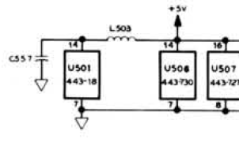
Also notice that U501 has a slightly different power supply arrangement to the bulk of the other ICs:

1692260788460.png
Because of the high frequency oscillations involved, the designers did not want this feeding back through the power rails of U501 to everything else. They therefore installed indictor L503 and capacitor C557 to minimise this. If either L503 is going open circuit - or C557 is going open circuit or short circuit - then this will have a major effect on the crystal oscillator.

Dave
 
Last edited:
I'll do the voltage measurements on P516 with the scope and let you know the results. I certainly have tantalum capacitors that haven't been changed yet. Should I change them out first?
 
They are usually the culprits...

It is much easier if they go BANG... But they can also go low resistance, push the current consumption up and may reduce the rail voltage as a result.

Dave
 
I measured the AC noise at 20 MHZ. Not sure how to measure it at 60, 100, or 120 HZ. I'll have to go through my manual. I'm not a scope expert at any means. The noise was .01 mv p-p with a 50-ohm load. Sounds crazy to me. I measured this right off the U101 5-volt regulator. It didn't make any difference whether P516 was plugged in or not. There was a lot of difference when I measured the DC from U101 using a multimeter. It was a strong 5.1 volts without P516 being plugged in. When it's plugged in it measured from 4.64 to 4,24 as the voltage slowly decreases over time. I'll try to figure out the noise at a lower frequency. Does it need the 50- ohm load added by the scope? Wish I was smarter. Thanks.
 
No need for a load, just stick the oscilloscope probe across the power rail you are measuring - 0V and (say) +5V.

You only need a load resistor on a power supply if it is not plugged into the logic board (i.e. the power supply does not have a load).

On a logic board I usually measure on a few IC power pins scattered around the board and take the worst reading.

The low frequency noise comes from the power supply - especially from failing smoothing capacitors on a linear supply. These are the very large electrolytics you can see.

High frequency noise comes from the logic ICs switching, and is induced into the power rail. The purpose of the little 0.1 uF decoupling capacitors (that should be spread over the board) is to provide a 'pulse of charge' when an IC switches. This limits the noise. However, if these capacitors are dying (going open circuit), this 'pulse supply capability' will diminish, and the noise will increase.

To measure the low frequency noise, you just slow down the oscilloscope timebase... For example, to measure the noise at 50 Hz. 50 Hz has a period of 20 milliseconds. So setting the oscilloscope to a timebase of 20 milliseconds/division will capture 1 cycle of 50 Hz noise for every 1 division of the oscilloscope timebase. Simples...

This works for higher frequencies too. 1 MHz = a period of 1 us, so a timebase of 1 us/div will be ideal.

If you find anything of interest, just expand the timebase to examine it further.

An even simpler way is to just 'sweep' the timebase from the slow end of the scale to the high end and see what you see!

You may find a X10 setting on your probe (if you have one) better than X1 (but don't forget that your voltage reading on your oscilloscope has also reduced by a factor if 10, so you have to compensate by MULTIPLYING any oscilloscope voltage reading you obtain by 10).

Also, don't forget to select AC coupling to read the noise and get the noise to fill the screen (in the Y direction) before taking a reading. The clue is that there is ALWAYS noise present. The question is "how much"?

Dave
 
10 uV pk-pk noise is somewhat optimistic I am afraid!

The DC voltage drop when plugged in is a little concerning.

Where are you actually measuring the 0V and +5V when plugged into the logic board?

The cables could be damaged or the connector could have gone high resistance. Measure the voltage directly at the output of the +5V regulator (U101) with the PSU connected to the logic board. This goes for the 0V connection to the scope as well. Connect it to the 0V rail of the PSU NOT the logic board to start with.

If that is OK, you can move the meter to both sides of connector P516. Pin 2 (0V) pin 3 (+5V).

Basically, follow the power from the +5V regulator to the PSU-side of P516 then the logic board side of P516 to see where the voltage starts to disappear...

You can also measure the DC voltage at the input to the +5V regulator U101 - to see if this voltage is collapsing when loaded.

If the voltage is falling, this could be due to something faulty (but we need to identify where we need to concentrate our effort). It could also be an excessive current flow in the +5V rail. We will need to measure what the current consumption is in this case with your meter (if we can).

Dave
 
Last edited:
10 uV pk-pk noise is somewhat optimistic I am afraid!

The DC voltage drop when plugged in is a little concerning.

Where are you actually measuring the 0V and +5V when plugged into the logic board?

The cables could be damaged or the connector could have gone high resistance. Measure the voltage directly at the output of the +5V regulator (U101) with the PSU connected to the logic board. This goes for the 0V connection to the scope as well. Connect it to the 0V rail of the PSU NOT the logic board to start with.

If that is OK, you can move the meter to both sides of connector P516. Pin 2 (0V) pin 3 (+5V).

Basically, follow the power from the +5V regulator to the PSU-side of P516 then the logic board side of P516 to see where the voltage starts to disappear...

You can also measure the DC voltage at the input to the +5V regulator U101 - to see if this voltage is collapsing when loaded.

If the voltage is falling, this could be due to something faulty (but we need to identify where we need to concentrate our effort). It could also be an excessive current flow in the +5V rail. We will need to measure what the current consumption is in this case with your meter (if we can).

Dave
Thanks for the good advice, Dave. I am measuring the 5 volts directly from the 5-volt regulator at all times. The 0-volt pin of the scope is not connected to the logic board but the power supply ground. Yep, I'm getting 5.1 volts directly from the power supply when P516 is not plugged in and around 4.35 volts when it is plugged in. The VCC reading at U502 is about 4.30. What should be an optimal noise reading at low frequencies? Thanks. I think I will change out the capacitors in this circuit when I can get them. What do you think?
 
Thanks for the good advice, Dave. I am measuring the 5 volts directly from the 5-volt regulator at all times. The 0-volt pin of the scope is not connected to the logic board but the power supply ground. Yep, I'm getting 5.1 volts directly from the power supply when P516 is not plugged in and around 4.35 volts when it is plugged in. The VCC reading at U502 is about 4.30. What should be an optimal noise reading at low frequencies? Thanks. I think I will change out the capacitors in this circuit when I can get them. What do you think?
I should note that if the voltage is dropping as much as you say, the regulator would be hot enough to make spit boil. If it is not that hot, it is a bad regulator. And yes, they can look to be working under a light load.
Dwight
 
Back
Top