• Please review our updated Terms and Rules here

Help with Commodore PET ROM Pager board

AndyG

Experienced Member
Joined
Oct 11, 2016
Messages
396
Location
UK
First time Posting on this forum though I have been following for a little while.

I have a PET 3000 series (well 2001-N) and it has an 8 ROM Pager board inside it with a ribbon cable connected to ROM $9000.

There also is a special edit ROM (called rather unhelpfully ROM-X 80066) but not sure if they are related (all I can detect so far with this ROM is I get auto repeat on any key I press though think there maybe more).

I have tried googling for info on the board but cannot really identify how to use it. I believe I need to use some POKE sequence but wondered if anyone has ever come across this and if so any idea how to work it ?

The best I can find that maybe similar, is an AD from Reprodesign Microcomputer systems (and reference to it in Getting More from your Pet)

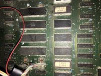
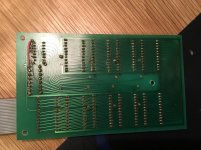
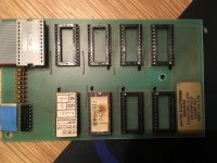
Pics of the board and ROM chip are attached (the connector on the UP doesn't do anything).
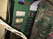
IMG_1503.jpgIMG_1504.jpg

I have posted on the Commodore.CA Forum and TPUG (apologies if you have already seen the thread!) but wanted to reach out to a wider audience as not sure if this is a UK Home Brew piece of kit or was available across a broader market.

Many Thanks in advance
 
I'm assuming all this does is let you bank ROMs, eliminating the need to plug them in one at a time to use them.

My best guess is that the ROM has a routine for selecting ROM banks on the separate board. Apparently it gives you key repeat, but it's anybody's guess what else.

If you could dump the ROM, we could probably figure it all out eventually.

Put some stickers over those EPROM windows before they get erased, if they aren't already.

What do the two stickers that are there say on them? One looks like a dongle for some software, most of the others probably are, too. One might be some kind of BASIC enhancement or something.
 
Thanks for the quick reply.

I have actually backed up each of the ROMS (taht are not covered) and reused them as I had a defective BASIC 2 ROM and also needed to create a standard BASIC 2 Edit ROM.

You are right about the ROMS on the board - one of the uncovered ones was BasMon, the other one (has 2K of code on a 4K chip) I don't know. The unlabelled chip on the Motherboard next to the Arrow ROM is actually the advanced programmers toolkit.

Can you guide me on how to send over the .bin file for the ROM-X ?

Just curious on how to drive the add-on board as the Ad suggested it was through a specific POKE but cannot find anything on the NET.

Cheers
 
Just curious on how to drive the add-on board as the Ad suggested it was through a specific POKE but cannot find anything on the NET.

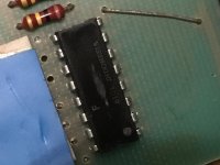
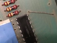
Usually there is a 8 position DIP switch to select the EPROM to be mapped to $9000 area. I only see a small IC and eight pull-up resisters to control this function. Is the chip a 3 to 8 decoder? Even then, it would need to latch the decoded information. The chip is too small to be a PAL logic device which could perform this function. What is the part number on the small chip?
 
Um, no dip switches. Uploaded more pictures as this is now making me very curious.

The ic has F 8101 written in it.... I think.

IMG_0942.jpgIMG_0945.jpgIMG_0941.jpgIMG_0943.jpg

Thanks for your replies

Andy
 
January 1981. It looks like the part number has been scraped off. I agree with Dave, it looks too small, but, it almost has to be. (It can't be; there aren't enough pins.) Or there's something we're not seeing here.

What's on the other end of the ribbon cable?
 
Ribbon cable goes to a 24 pin connector that went into the Rom socket on the PET motherboard. There's nothing else plugged in internally, other than an Audiogenic PETSET 2 part reset switch board (now connected to NMI and Pin 22 on the expansion port) and an in built amp/speaker... that's what the red wire is there for when you look at the motherboard.

Something must be missing as you gotta be able to select the appropriate ROM somehow. It has been a long time since I really messed about with the PET (first computer I cut my teeth on) ...
 
Last edited:
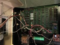
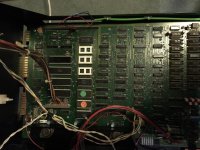
Pictures of the internals....

Was an 8k system upgraded to 32k.

IMG_0946.jpgIMG_0947.jpg
 
There was a couple of different cards made by this chap/company. See http://archive.6502.org/publications/icpug/icpug_v05_i04_jul_1983.pdf on page 338.

The writeup says either by a DILL switch (clearly not this model) or by software control.

Are we convinced it is actually plugged into a ROM socket and not a RAM socket in the PET?

If it was plugged into a RAM socket - then any write to the area could be taken, latched and decoded by the pesky chip whatever it is. I wonder if there were any small latch and decoders made?

I agree that the part number has been erased - what you are seeing is the date code.

EDIT: I think this board is required to be connected (via a short lead that is missing) to the USER PORT. I can see a link from pin 20 (?) of the ROM cable socket to the 16-pin chip. I suspect you select the ROM you want to use externally via a POKE to the USER port and this - in turn - connects to the 16-pin chip via some wires that are broken off. That's my gut feeling. I suspect that the 16-pin chip is just a 3->8 decoder (perhaps with open collector outputs - hence the array of pull-up resistors). It clearly isn't a 74138 - the pinouts don't look right.

Dave
 
Last edited:
Thanks Dave. That makes things a lot clearer and explains the presence of the User Port connector with nothing connected to it!

The board definitely connects to the ROM socket, and looking at the UP connector, there appears to be heavy blobs of solder on PA0, PA1 and PA2.

On the reverse side of the board there are two holes near the IC chip with reasonable amounts of residual solder on them and faint amounts on the the pin 20 line from the eprom ribbon cable connector to the chip. Also faint solder seen on the hole that is on the common rail to all pin 24 of the eprom chips.

The photos shown in previous post may show these better.

Got no idea how to wire this up ....
 
It would be worth chasing the PCB wiring out around the 16 pin chip so we can come up with a partial pinout.

For example, there will be eight outputs going to the pull-up resistors and on-board EPROMS. There will be one input coming from the /CE pin of the interconnector ROM socket.

There may be some pins tied high or low.

The remaining pins would probably be address lines from the user port.

From this it may be possible to search the old TTL data books to identify a suitable component that it may be.

The other way is to power up the board from an external power supply unit and test various combinations of logic levels on the pins by wiring up the 'broken' points to a simple DIP switch and resistors. By applying a multimeter to the unconnected pins it should be possible to deduce if they are inputs or outputs. If inputs - you could wire them up to a DIP switch and resistors. You could then use the 'trial and error' method to find out what selects each ROM. Having identified the address and enable lines - you can then wire these to the PET's USER port and you would be good to go.

Sounds easy to say - but if you are interested in getting this card operational I could provide some more details for you regarding how I would go about it. No guarantees though :)!

I guess you are in the UK. Where? I am in Worcester.

Dave
 
The other way is to power up the board from an external power supply unit and test various combinations of logic levels on the pins by wiring up the 'broken' points to a simple DIP switch and resistors. By applying a multimeter to the unconnected pins it should be possible to deduce if they are inputs or outputs. If inputs - you could wire them up to a DIP switch and resistors. You could then use the 'trial and error' method to find out what selects each ROM. Having identified the address and enable lines - you can then wire these to the PET's USER port and you would be good to go.

Dave,
He could also just replace the IC with a DIP switch and manually select the EPROM.
 
They did sell a DIP switch version. I would prefer to get it working properly ..... I live down the road in East Anglia :D

I have to confess I am getting a little out of my depth now (programming or replacing IC components etc .. not a problem) but willing to have a go.... :)

Will also contact original owner to see if they have any documentation but not holding out for success on that front.
 
Trying to get it working properly should not require replacing any components - just a bit of soldering to re-attach the user port cable.

Programming just consists of the right BASIC POKE statement(s) to select the correct address of the EPROM required on the USER port - nothing more. It is the same sort of POKE required to light some simple LED's connected to the USER port - so it is a worthwhile exercise to get some pretty LED lights working from your PET...

I was just about to print out your photograph of the rear of the PCB and trace it out over the weekend. If you could take a better photograph of the rear of the PCB (in nice bright light and square on so you can see all of the individual PCB tracks) that would be better for me though...

East Anglia - turn right and keep going until your feet get wet if I remember correctly...

Dave
 
Will take some tomorrow in day light - many thanks Dave ....

Yes, I remember at college all those years ago the electronics dept made a LED box which I wrote a few programmes for - (Knight Rider style :eek:) !


Andy
 
Of course Dave...

Andy,

Solved it...

I think your mystery IC is an SN7445 BCD to decimal decoder with open collector outputs.

IC pins 1-7 are decoded outputs 0-6 with pins 9-11 being decoded outputs 7-9. Of course, only decoder outputs 0-7 are actually used for the 8 EPROMS. Please note that not all EPROMS are inserted the same way round! Someone has kindly marked pin 1 of each EPROM with a black felt tip marker pen for you I see!

The missing part of the equation (to drive the thing) are the three broken wire inputs going to pins 15, 14 and 13 of the IC. These are the least significant bit (pin 15) to the most significant bit (pin 13) of the 3 bit EPROM selection input. The most significant BCD input bit (pin 12) is internally wired to pin 20 of the 24-pin ribbon cable connected to the PET's ROM socket.

You would need to wire the three (3) broken wires to the three least significant bits of the USER port - or to three switches (or a DIP switch) and a few pull-up resistors from Maplin as a test rig.

I would suggest downloading the SN7445 data sheet (e.g. http://www.ti.com/lit/ds/symlink/sn7445.pdf) and have a read of it first to see if it makes sense...

I can help you further when I get back next week.

Dave
 
Get it working properly...

I would improve on it. I'd add a PIA or VIA and some address decoding. It seems a great waste to tie up the user port.

Although really, what I'd probably do is use a rotary switch outside the PET case. The only advantage to programmable switching is that a very serious programmer could use ROM routines from multiple ROMs. Even I don't think I would need that on a PET, though.
 
Back
Top