• Please review our updated Terms and Rules here

IDE hard drive on an IBM PC Convertible

It is interesting how that’s put together; it looks like it uses the same female connector that mates to the expansion bus externally as the “slot” for that board. I wish they’d used the female end on the system unit instead of the male, then we’d be on easy street. (Comparatively speaking.) Presumably that connector was available commercially at some point for that third party to have laid hands on it...

So I suppose if you have a spare system unit and a gut-able spare slice I could try taking a shot at it, I’ve been looking for another project? The available board area looks similar to the 100x100mm Tandy Plus Cards I’ve made and I was able to get a CF-Lite and a dual serial port combo into that space, although I’ll also need to factor in the address latches. (Fitting the original case plastics might be a challenge. If that’s not feasible could still make it work by salvaging the connector module only and looking at 3D printing a new shell?)

The original docs for the parallel/serial slices discuss the system having a simple “plug and play” system where the slice has a configuration register that is set by the system setup program to adjust the device address. I wonder if that’s necessary for a serial port to work or if hard decoding at the right address would be sufficient. It looks like that slice has any configuration register magic locked up in that ASIC, the discrete hardware on it doesn’t amount to much.
 
I also took apart the display slice I have. It has the same connector for the bus, but there are two circuit boards laid on-top of each other, about 1/4" apart, connected by what looked to be a pretty standard pin/socket connector. By comparison the serial/parallel slice only has that single board in it, and there is definitely enough space in there to layer on a second PCB if need be.

Yes, I have a 5140 you can play with, and a slice you can dissect. I gather you are in the South Bay? I work near Stanford, so PM me and maybe we can find a place to meet up in that area.
 
Yes, I have a 5140 you can play with, and a slice you can dissect. I gather you are in the South Bay? I work near Stanford, so PM me and maybe we can find a place to meet up in that area.

PM sent.

Are the boards really only 1/4" apart? That's tight. Surface mount? (The standard .1" pitch headers like the ones Plus cards use sit the boards about 1/2" apart, which is enough for socketed through-hole but just *barely*.)
 
Are the boards really only 1/4" apart?

Err, maybe not. That was just a guess, but now that I look at a ruler it was more like 1/2" - 3/4" Opening up that slice was a PIA, so I won't do it again. My main point was that there is a lot more space in the slice than the pictures would lead you to believe, and if a single PCB is not enough, then doing a sandwich of 2 could work.
 
Last edited:
Err, maybe not. That was just a guess, but not that I look at a ruler it was more like 1/2" - 3/4" Opening up that slice was a PIA, so I won't do it again. My main point was that there is a lot more space in the slice than the pictures would lead you to believe, and if a single PCB is not enough, then doing a sandwich of 2 could work.

Ah, So yeah, it's probably just a standard header, so that's potentially great. Getting an IDE port *and* I/O ports on a single board was looking tight, but if I could do a sandwich that problem should go away. I wonder if it's worth tossing a RAM chip in there to get UMB memory as a bonus. (It's easy to share the decoding for a ROM chip, just need room for two big DIPs instead of one.)
 
Last edited:
Did any progress get made on this? I've always loved the 5140, since first playing with one, not long after they were released.

I also have a fully functional 5140, that I've been playing with.

- Alex
 
Did any progress get made on this?

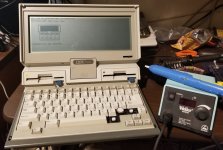
So I guess it depends on how you define "progress". I have gotten my grubby talons on a 5140. Unfortunately it's a... ridden hard and put away wet specimen. I haven't had a lot of time to work with it yet but I did spend a few hours this last weekend trying to at least get it running:

convertible-sml.jpg

The keyboard is really badly shot; I have all the keys at least registering now, enough were completely dead that I couldn't really uses the machine (letter G, number 3, period...), but it took some soldering. The ALPS keyswitches in it are pretty badly corroded and I'm not sure if they're the stock ones or if someone swapped the ones that are in there for more desirable originals? Solder joints on the keyboard's PCB are kind of suspiciously bad. The machine is still hanging at random sometimes, especially when accessing the B floppy drive. Hopefully I can get the kinks smoothed down enough to feel like I can trust trying to engineer something with it.

I haven't had a chance to crack open the parallel-serial module and start buzzing the connections to its internal card edge yet. I assume they're mostly mapped 1:1 with the back-edge connector but they could be swapped/mirrored. If anyone out there has a line on the female mating connector for the modules so I could target that directly that would still be awesome.
 
Picking up this thread again after a lengthy hiatus...

Anyone got an accurate photo? Maybe I can help.

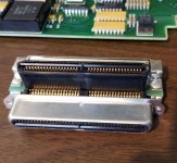
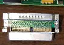
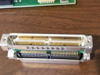
I finally got around to cracking open the parallel/serial slice for an IBM Convertible. The slice contains a circuit board with an edge connector that plugs into this weird little splitter assembly that has two of the connectors that would be *really* nice to be able to find, in two versions.

The heart of the connector is a circuit board which makes up the male passthrough connector, which has a total of 72 contacts split into two 2x18 sections. The female connector facing the computer is soldered to what looks like an identical card edge using a version of the connector that has two rows of inwardly canted fingers, while the female connector that faces upwards is through-hole with four staggered rows of pins.

Unless I miscounted twice pitch of the connectors appears to be about 16 contacts per inch. I've completely failed to turn up any hits for any standard or metric translation of that I could come up with. This whole assembly appears to have been made by one company, the female connectors have molded into them the same double-sided "P" / slash / badly made pretzel logo you can see on the bottom of the PCB. Here's some pictures.

whole.jpgtop-orientation.jpgbottom-orientation.jpgend-orientation.jpg

If anyone has any hint as to where a batch of the female connectors could be had (I'd settle for either the edge-on or the through hole) that's be awesome.
 
Last edited:
Pretty cool thread. Was curious if anyone else documented one of these. It came with a 5140 someone gave me back in 2019, and the crappy Miniscribe it came with worked (then). Guess I get to see if it works this morning.
 
Back
Top