• Please review our updated Terms and Rules here

Memory problem with PET 2001

There could be a timing concern here but my limited understanding is by no means correct.
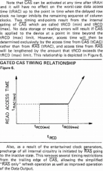
* "Operation within the tRCD (max) limit insures that tRAC (max) can be met. tRCD (max) is specified as a reference point only if tRCD is greater than the specified tRCD (max) limit, then access time is controlled exclusively by tCAC."
Likewise welcome! Don't let the initial moderation posting delay put you off, it wears off after a bit.
In the super slow PET the timing is much larger than the DRAM device allows so I don't think these constraints matter... or more precisely the nCAS (i.e. tCAC) does drive and it operates in a mode >> tRCD.

Thank you!

Greg, is it possible to get traces showing only read and only write cycling, for additional comparison? And I read you replaced most ICs but are these OG MOSTEKs? (I am skimming TI spec sheets also.)
 
Going to artificially inflate my postcount a bit to get out of this mod jail...

The negative LSL for tCRP was bothering me before ( left it grey ) and, while researching a bit more, it seems others have had timing concerns with mixing separate eras:
* https://retrocomputing.stackexchang...16-have-a-negative-column-address-set-up-time

Regarding mux, is there a way to measure voltage and determine "precharge" timing or am I missing this information in an earlier oscope post?
* "The bit-line sense amps and wide column select mux had to consist of a large total gate area. Thus it would take quite awhile to precharge all of that. The column address would not be needed to pull down some selected gate path until after the precharge completed, This might take up most or all of that 20 nS using NMOS transistors that were several square microns in gate area. The column address thus need not be latched until after the end of the precharge pulse that was perhaps triggered by the falling edge of CAS."
 
You need about 10 posts...

From the trace back in post #123 I think we concluded that address $0000 was OK and things started to fail at address $0001.

From that trace I believe I could see a '1' being transiently written (erroneously) into D7 during the write cycle.

From post #133 trace #1 I think that was confirmed - but trace 2 (testing address $0000 only) was fine.

Two possibilities now present themselves:

1. Use the simplified code that we used for testing memory location $0000 out alone and modify that to use page 0 address $0001 and see what happens.

2. Start to look at the /RAS, /CAS and MUX timing. We have already looked at the 8-phase generator - but we may need to look a bit more closely at the subsequent timing logic.

I would propose we perform option 1 first - as the logic analyser is already set-up.

First use the sample code we had back in post #110.

Modify the following instructions and retest:

Where we had two (2) instances of

Code:
STA 0
LDA 0

Change to:

Code:
STA 1
LDA 1

Testing the code first with address $0000 should give us the same trace as in post #133 trace 2 (for comparison and check purposes).

Then modifying the code to use address $0001 should give us another trace for comparison.

All you need to do to change address $0000 to $0001 is to patch the second byte of each of the four (4) instructions from a $00 to a $01. The high byte of the address is assumed to be $00 because we are using page zero addressing mode.

Sound sensible?

If this indicates a timing problem - we can then move on to look at the DRAM control signals and logic.

Dave
 
Last edited:
Sound sensible?
Always. :D
The only other thing I wondered about is... if the row/col address muxing is the problem... then maybe we need to see MUXA in the analogue domain on a scope... the LA might be squaring things up in a way that might throw us off... but in the context of $0001 might be even better.
 
I'll take a few more traces of read and writes blown up for additional comparison.

Most of the original ICs on PETs were, thankfully, not made by MOS. The PET uses almost all standard 74-series logic chips. MOS's versions of these were almost without exculsion, terrible. In the several C64s I've repaired I don't think I've ever actually seen a still-working MOS logic chip. Thankfully, I don't think they were really making these in 77 or 78 when this PET was built. My understanding was that they started making them as a hedge against other suppliers to get the pricing they wanted for the C64. I could be wrong. Has anyone seen a PET with MOS parts?

The parts I've been replacing things with are TI, Motorola and National Semiconductor for the most part, all pretty solid vendors. The majority of what I took out were TI and I believe National Semiconductor. The DRAMs were Hitachi. Interestingly the TI parts seemed to rust very badly compared to the others. Hopefully that won't be a problem in the future since I plan to keep this machine in a better environment than the last owner (in a shed, near a salt water inlet.)

Greg

Thank you!

Greg, is it possible to get traces showing only read and only write cycling, for additional comparison? And I read you replaced most ICs but are these OG MOSTEKs? (I am skimming TI spec sheets also.)
 
Last edited:
Alright, exciting!

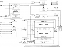
If there is both a timing and MUX concern, could that point to the root cause hiding in ( at least ) Clock Generator No. 1?
Func Diag.png
 
Likewise welcome! Don't let the initial moderation posting delay put you off, it wears off after a bit.
In the super slow PET the timing is much larger than the DRAM device allows so I don't think these constraints matter... or more precisely the nCAS (i.e. tCAC) does drive and it operates in a mode >> tRCD.

Thank you I am starting to understand more as I get through the memory design document.
Untitled.png
 
I think I may have this problem licked. I know Dave doesn't like swapping stuff randomly, but based on the fact that 1. We were pretty sure that the problem was timing-related and 2. I knew that I had faster LS parts in some locations that call for S or standard 74 parts on the schematics, I went ahead and replaced the 74LS74 I had in location H1 with a newly received 74S74. I put in the PETTESTER ROM and let it run without issue through 64 passes of the memory test over the course of about 2 hours without any errors.
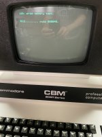
IMG_7242.jpg

Should I be satisfied that this is now working properly? Are there any other tests that I should do or should I just use it and see if anything crops up. I'm more than happy to do any other tests and measurements that you can suggest to verify operation or to wrap up any of the threads that we were discussing. I've retained the part and can easily swap it back in for comparison.

But, if there's nothing else to be done, I just want to make sure I thank you all for your help -- especially Nivag and Dave. I definitely owe you many beers or whatever other libation is to your liking. I hope maybe someday I'll get the chance to pay you back on that.

Also, I wanted to get a general feeling from the group as to whether I should upgrade the RAM from 16k to 32k. The pads are all present on the board and I have enough memory on hand to do it. The board is already very much not original from all the rework I've had to do to get to this point, but it's more-or-less equivalent to what it would have shipped with. Any opinions?

Cheers,
Greg
 
Last edited:
>>> I know Dave doesn't like swapping stuff randomly, but

It worked, so I would take it!

Good to see that it passes my PETTESTER code (that is a pretty stressful test). However, I would still try our walking ‘1’ test just to make sure that doesn’t identify something awry.

Since you now have a socket in there for the 74x74 (H1) I would take s logic analyser trace (with the walking ‘1’ test that you have previously validated still works) to check what has happened to ‘fix’ the timing.

The worst case scenario here is that you are masking the problem by changing H1 rather than fixing the problem. If it was borderline erroring before, it may be borderline working now?

I will take a look at the schematics on Monday. I have another project to do today (housework)...

If you are going to keep the PET for your own purposes then I would upgrade to 32K (to run larger programs). But use IC sockets of course just in case the upgrade causes problems... But’s that only my opinion of course...

Dave
 
Wow! Well I wasn't expecting that! 74..74 devices are notorious in their failure like ...161s etc but I was NOT looking in that part of the circuit!

Now... We should have spotted that on a scope picture of nRAS0... might have to look back.

The fundamental difference between a 74LS74 and a 74S74 is output drive. A 74S74 can pull down 20mA whereas a 74LS74 can do less than half that!

For my own amusement I would want to see a scope trace of nRAS and MUX together with old and new... I suspect you might find the relative timing might have a slight difference.

But.. don't chase red herrings down rabbit holes... a win is a WIN!

Good job
 
Last edited:
The timing should be locked to a clock pulse (one of the 8 phases) and not left to the whim of a gate delay or pull-down capability.

At that frequency - any type of 'slow' gate should really work IMHO.

I suspect we have not fixed the fault - only masked it - unless H1 really was 'dead ish'.

You may find (for example) it is really H2 or H4 - and putting a faster gate in place of H1 has just shifted the errant pulse slightly to the left or right (thus masking the problem only for it to reappear again as the machine continues to age further).

Just a thought - but I would still have a play with the machine myself to check out more of the functionality to make sure other things are OK (e.g. does it now run BASIC and does the cassette interface work).

Dave
 
I finally got a little quality time with the PET tonight. I took some traces with the walking bit test. Here is an example of it when it is writing a "1" to RD7 at address $00 and reading it back.
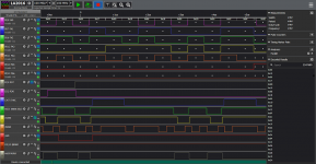
RAM_addresses_control_ok.PNG
To my eye, this looks correct.

I've also played around with the machine quite a bit. It boots to basic, I can type in programs and the run, etc. I haven't tried loading things from cassette as my datasette needs to be serviced. I have successfully loaded things from "disk" (PET2SD) repeatedly with success and played a few games, etc., that all seem to play and run normally (although sometimes the keybindings are weird, presumably because I have a business keyboard and the games don't take that into account.) No random drops into the ML monitor or anything. It currently seems to be 100%.

I also installed 8 new sockets to upgrade the RAM to 32k. However, I haven't been able to get the second bank of RAM to be recognized correctly, at least by BASIC. I think this is probably because of the jumper settings. Here is a photo of the two jumper blocks as they are now, working properly with 16k of RAM:
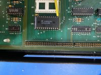
IMG_7245.jpg
Pretty nasty and rusty looking, I know, but has good continuity across all the unbroken links. BTW, this is how basically every IC on the board looked when I started working on it. I haven't touched these since I thought the type of jumper was interesting and knew I can't replace them. By eye and by my meter, this is how they're configured:

A: open
B: open
C: shorted
D: open
E: open
F: shorted

H: shorted
I: shorted
J: shorted
K: open
L: open
M: open
N: open
P: shorted
R: open
S: shorted

If we compare refer to the documentation at http://www.zimmers.net/anonftp/pub/cbm/schematics/computers/pet/2001N/320351-6.gif, the jumpers when used with 4116 RAM (the mentioned item 33) should be set like this:
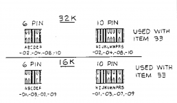
jumper_settings.png

Neither the 16k nor the 32k configuration correspond to what I have on my board, working with 16k.

If we refer to jumper block in the RAM schematic at http://www.zimmers.net/anonftp/pub/cbm/schematics/computers/pet/2001N/320349-5.gif
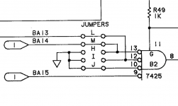
jumpers_schematic.png
This looks to me like maybe L and M should be open and H, I, and J should be shorted, which is how the board is set (for 16k) and what is indicated in the document for 32k. Other jumpers in the schematic and on my board (A, B, C, E, F) agree with the document. I can't find any of the other jumpers in the schematic (D, K, N, P, R, S), so no idea about those.

So, does any one know what the correct jumper settings for 16k or 32k are?

If I need to short any of these, does any one know if that's possible using these same blocks? Should I replace them with pin headers and regular jumper caps? Should I keep the jumpers as they are and if I need to short them should I just solder a bodge wire to the bottom of the board to keep these looking original?

Or, does it seem like it's not a jumper problem and I should start beeping out traces and looking at signals on the second bank of RAM?

Cheers,
Greg


>>> I know Dave doesn't like swapping stuff randomly, but

It worked, so I would take it!

Good to see that it passes my PETTESTER code (that is a pretty stressful test). However, I would still try our walking ‘1’ test just to make sure that doesn’t identify something awry.

Since you now have a socket in there for the 74x74 (H1) I would take s logic analyser trace (with the walking ‘1’ test that you have previously validated still works) to check what has happened to ‘fix’ the timing.

The worst case scenario here is that you are masking the problem by changing H1 rather than fixing the problem. If it was borderline erroring before, it may be borderline working now?

I will take a look at the schematics on Monday. I have another project to do today (housework)...

If you are going to keep the PET for your own purposes then I would upgrade to 32K (to run larger programs). But use IC sockets of course just in case the upgrade causes problems... But’s that only my opinion of course...

Dave
 
Last edited:
Yes, address $0000 looks fine. However, the interesting thing would be address $0001 (as stated back in post #164).

The fact that the machine appears to work consistently is good, I am just concerned as to why? That has never been answered (except by a faulty H1 that we don’t know that for sure).

Links N, P, R and S are on sheet #1 - and are nothing to do with DRAM.

The only link of concern is K. It is not on the schematic but should be linked. This could be a factory-fitted link and may not appear on the schematic due to an oversight?

I would probe around with a multimeter (power off) to see if you can find out where the two ends of link K are connected to.

You could also check with the scope that /CAS1 is being activated (along with BANK SEL) etc.

Dave
 
Last edited:
I didn't have time to hook the logic analyzer up to check $0001 yet, but I was able to get 32k up and working consistently. A couple of the (still original) RAM chips in the first bank didn't seem to want to play nicely with the newly added RAM in the second bank. I presume they must be marginal and the extra load on some of the lines caused them to not be as reliable. Swapping those out for new ones seems to have fixed the issue and it passes the memory test. The jumper settings on the board as listed above seem to work with 32k. I thought I had what link K does figured out, but in thinking it through in order to write it up here I realize I need to revisit the board.

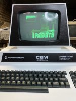
I was able to play "Attack of the PETSCII Robots", which requires 32k, for quite a while without trouble (other than sucking at the game.):
IMG_7254 2.jpg

I will take traces at $0001 with the logic analyzer and re-examine link K next time I get a chance to work on things. After that, I want to add CB2 sound and see how that works. I'll have to look at how some have implemented that and likely procure some parts.

Cheers,
Greg

Yes, address $0000 looks fine. However, the interesting thing would be address $0001 (as stated back in post #164).

The fact that the machine appears to work consistently is good, I am just concerned as to why? That has never been answered (except by a faulty H1 that we don’t know that for sure).

Links N, P, R and S are on sheet #1 - and are nothing to do with DRAM.

The only link of concern is K. It is not on the schematic but should be linked. This could be a factory-fitted link and may not appear on the schematic due to an oversight?

I would probe around with a multimeter (power off) to see if you can find out where the two ends of link K are connected to.

You could also check with the scope that /CAS1 is being activated (along with BANK SEL) etc.

Dave
 
For my own amusement I would want to see a scope trace of nRAS and MUX together with old and new... I suspect you might find the relative timing might have a slight difference.

Yea, same here, but also don't mess with it if the system is up and running!

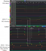
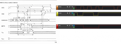
I stretched the latest plot and compared with earlier plots and MUX and CAS were a bit different ( and of course you were right about tRCD not seemingly mattering ). Are there any better timing plots to use as a reference?

Could the memory the PET had, as received by Greg, be from production early on and of not so great a design copy?

Compare_sm.png
Write_cyc_early_sm.png
 
You may find (for example) it is really H2 or H4 - and putting a faster gate in place of H1 has just shifted the errant pulse slightly to the left or right (thus masking the problem only for it to reappear again as the machine continues to age further).

Dave

This is all very new to me; what changes have you seen as the boards and ICs age?
 
Back
Top