| VCF West | Aug 01 - 02 2025, | CHM, Mountain View, CA |
| VCF Midwest | Sep 13 - 14 2025, | Schaumburg, IL |
| VCF Montreal | Jan 24 - 25, 2026, | RMC Saint Jean, Montreal, Canada |
| VCF SoCal | Feb 14 - 15, 2026, | Hotel Fera, Orange CA |
| VCF Southwest | June, 2025 | University of Texas at Dallas |
| VCF Southeast | June, 2025 | Atlanta, GA |
-
Please review our updated Terms and Rules here
You are using an out of date browser. It may not display this or other websites correctly.
You should upgrade or use an alternative browser.
You should upgrade or use an alternative browser.
Model 1 Help
- Thread starter joeatact
- Start date


ldkraemer
Veteran Member
With Power OFF, Depress the BREAK KEY, and keep it depressed. Turn on POWER.
When you see any text on the Screen RELEASE the BREAK KEY, and Press the
ENTER KEY twice.
Do you see MEMORY SIZE or MEM SIZE?
The second photo shows the display to be in 32 character mode vs 64 characters.
Larry
When you see any text on the Screen RELEASE the BREAK KEY, and Press the
ENTER KEY twice.
Do you see MEMORY SIZE or MEM SIZE?
The second photo shows the display to be in 32 character mode vs 64 characters.
Larry
Eudimorphodon
Veteran Member
Just a bit of advice to the OP; it might be better for everyone if you organized all your questions into a unified thread describing what you have and what's wrong with it. This piecemeal approach you're taking to asking isolated questions about very specific technical details out of the blue makes it really difficult to follow what's going on here. (I mean, I assume you're asking here about the same machine in these two other threads.)
No. That's not likely to have anything to do with this behavior, especially if you're testing the machine without anything plugged into the expansion connector. (Although I guess if you want to talk about it, is this the only mod that's present, or does this computer also have a 5-pin DIN plug dangling out of the expansion slot hole that's connected via a few tack soldered connections to various places on the board? This would tell you if your keyboard had actually at some point in its life been paired with an expansion interface that required a specific set of hacks to work reliably.) What that mod does is convert a pin (39) that in the original Level I configuration provided a *very* current limited +5v output into a ground; Radio Shack did this mod by default on any machine they upgraded to Level II BASIC and it's expected to be there for any type of expansion interface. The only potential for problems is if you connected your keyboard to an expansion interface that needs the buffered cable with a plain cable. That would short the power that's fed to the buffered cable *from the expansion interface* to ground on the TRS-80. (The buffered cable isolates them.)
Anyway, regarding the photos of the screen you're showing, is that photo of the power-on state accurate, IE, does it really have those black drop-outs instead of complete characters? That would be very strange behavior because the TRS-80 screen hardware shouldn't need any software initialization to just spit out whatever random junk is in video memory when you turn it on. Are there flickering black streaks moving through the frame or other "dynamic" activity before you hit reset?
This would mean the bit on port FF that controls whether video is in 64 or 32 bit isn't being forced to zero... which would certainly imply that the machine isn't executing the BASIC ROM, since outputting a zero on that port is one of the first things the ROM does on power on/reset.
Based on the discussion in the other threads it kind of smells like your BASIC ROMs might be dead or non-functional, although I'm still not sure what to think about those black areas in the power-on photo. Maybe there's something broken with the timing chain and the CPU isn't even running, although I'm not sure why reset would change things...
There is a mod made for it to work with an old style e/i. Problem?
No. That's not likely to have anything to do with this behavior, especially if you're testing the machine without anything plugged into the expansion connector. (Although I guess if you want to talk about it, is this the only mod that's present, or does this computer also have a 5-pin DIN plug dangling out of the expansion slot hole that's connected via a few tack soldered connections to various places on the board? This would tell you if your keyboard had actually at some point in its life been paired with an expansion interface that required a specific set of hacks to work reliably.) What that mod does is convert a pin (39) that in the original Level I configuration provided a *very* current limited +5v output into a ground; Radio Shack did this mod by default on any machine they upgraded to Level II BASIC and it's expected to be there for any type of expansion interface. The only potential for problems is if you connected your keyboard to an expansion interface that needs the buffered cable with a plain cable. That would short the power that's fed to the buffered cable *from the expansion interface* to ground on the TRS-80. (The buffered cable isolates them.)
Anyway, regarding the photos of the screen you're showing, is that photo of the power-on state accurate, IE, does it really have those black drop-outs instead of complete characters? That would be very strange behavior because the TRS-80 screen hardware shouldn't need any software initialization to just spit out whatever random junk is in video memory when you turn it on. Are there flickering black streaks moving through the frame or other "dynamic" activity before you hit reset?
The second photo shows the display to be in 32 character mode vs 64 characters.
This would mean the bit on port FF that controls whether video is in 64 or 32 bit isn't being forced to zero... which would certainly imply that the machine isn't executing the BASIC ROM, since outputting a zero on that port is one of the first things the ROM does on power on/reset.
Based on the discussion in the other threads it kind of smells like your BASIC ROMs might be dead or non-functional, although I'm still not sure what to think about those black areas in the power-on photo. Maybe there's something broken with the timing chain and the CPU isn't even running, although I'm not sure why reset would change things...
Someone
Experienced Member
Not bad. Partial signs of life!
ldkraemer
Veteran Member
You can attach a Photo to your posting or direct message. You will likely have to email it
to yourself, so you can get it saved on your Computer, assuming you post using your
computer.
Larry
to yourself, so you can get it saved on your Computer, assuming you post using your
computer.
Larry

ldkraemer
Veteran Member
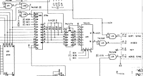
To check the address lines, remove the DIP Shunt at position Z3 and power-up the system. If the screen fills with a pattern
of “@9@9@9@9...”, then all the address lines A0 – A9 are good. The remaining address lines A10 – A15 can be checked
for activity with a scope.
Here's why you get @9s. With the ROMs removed, the CPU reads all 1's (that is, hex FFH) whenever
it reads from the area the ROMs are supposed to be in, because an open connection tends to
float to a 1 with this type of logic. Hex FFH is the RST 38H instruction. So when the processor is
turned on and fetches an instruction from 0000, it gets a RST 38H (FFH). This makes it push 0001
on the stack and jump to address 0038. At that address it reads another FFH, so it pushes 0039 on
the stack and jumps to 0038 again. Now it's in an infinite loop. As the loop continues, the stack grows
and grows, going backward through memory. When it reaches the frame buffer between 3C00 and 3FFF,
you can see it on the screen. It looks like a string of @9's because the TRS-80 displays a 00 byte as an
@ character, and 39 is an ASCII 9.
So, you need an O'scope to check the Address lines. You can make a NOP detector by using a SPARE
Z80 CPU, and Bending Z80 Pins D0 thru D7 up so they do go into the Z80 IC Scoket. You must Jumper
D0 thru D7 to the GND Pin of the Z80 CPU so it gives a 0x00 to the CPU, which will toggle A0 at
at the Clock frequency, A1 at 1/2 the frequency of A0 and on until around A9. This should locate your
problem as you can chase A0 thru A9 all over the Motherboard, looking for missing signals.
Larry
cjs
Veteran Member
Oh, I'd never thought of using this technique for debugging motherboards. Cute. But why does it stop around A9? I would have thought that even A15 would be toggling at around 5-8 Hz.You must Jumper D0 thru D7 to the GND Pin of the Z80 CPU so it gives a 0x00 to the CPU, which will toggle A0 at
at the Clock frequency, A1 at 1/2 the frequency of A0 and on until around A9. This should locate your problem as you can chase A0 thru A9 all over the Motherboard, looking for missing signals.
Someone
Experienced Member
If you're testing with %FF's it's best to weakly pull up the data lines via resistors to VHigh to prevent the bits from changing.
Likewise for NOP %00 testing but pull down to ground.
The last thing one wants to do is tie the data lines directly to GND or VCC.
Likewise for NOP %00 testing but pull down to ground.
The last thing one wants to do is tie the data lines directly to GND or VCC.
cjs
Veteran Member
Note that this is not necessary for Idkraemer's suggestion: the CPU data lines in that case are not connected to the motherboard at all, so when driven to $00 the CPU will just execute NOPs and will never try to drive its data bus pins. (Or so it seems to me; corrections welcome!)If you're testing with %FF's it's best to weakly pull up the data lines via resistors to VHigh to prevent the bits from changing.
Likewise for NOP %00 testing but pull down to ground.
The last thing one wants to do is tie the data lines directly to GND or VCC.
ldkraemer
Veteran Member
cjs,
I was going from my memory, which was incorrect, as it should have been A7. Here is why,
along with a bit more detail.
When a Z80 is hard wired for NOP's the refresh address (A0-A6) will always be the
same as the low 7 bits of the instruction fetch address. So, what you see on A0-A6
is double the duration of the instruction fetch. A7-A15 will go low each and every
refresh cycle. So, the effect of it all is A0-A6 will have a square wave with a
50/50 duty cycle. A0 will have a pulse length that is double the clock, A1 4 times
the clock etc. However, A7-A15 do not follow that pattern because the refresh address
counter is only 7 bits.
DATA LINES:
Absence of RD* and WR* will cause garbage on the screen. Any data line without activity
will also cause garbage. Remove Z3 and look at the display. An inactive data line will
often cause a pattern on the screen like @1@1 or Y9Y9 and the bad bit can easily be
found. Since the correct pattern is @9@9, the stuck bit can be determined mathematically
(similar to bad address lines above, subtracting the binary of @ or 9 from that of the
character seen). The most common cause of a stuck data line is a bad memory chip, the
inputs of which are tied directly to the data lines. Removing all memory chips and
checking the pattern will identify whether the problem is RAM or some other chip.
VIDEO RAM:
Ram errors are the most common video problem. To isolate the defective chip, first
determine the ASCII code of that character that should be shown and the character that
appears instead. For example, a blank screen (press CLEAR) is filled with ASCII code
32's (the code for a “space”). If some location shows a “$”, which is ASCII 36, subtract
36-32=4. The location with the error is displaying character 36 instead of character 32
because bit 2 is stuck on (2^2=4). Replace Z46. Similarly, if pressing “B” on the
keyboard displays “J” on the screen: B=66, J=74, 74=66=8, and since 2^3=8, replace Z45.
Larry
cjs
Veteran Member
Ah, I'd totally forgotten about the Z80 refresh cycles. So we won't be seeing square waves on A7-A15. But we will still see an AC signal on those, right? Which still seems good enough for debugging.When a Z80 is hard wired for NOP's the refresh address (A0-A6) will always be the
same as the low 7 bits of the instruction fetch address. So, what you see on A0-A6
is double the duration of the instruction fetch. A7-A15 will go low each and every
refresh cycle. So, the effect of it all is A0-A6 will have a square wave with a
50/50 duty cycle. A0 will have a pulse length that is double the clock, A1 4 times
the clock etc. However, A7-A15 do not follow that pattern because the refresh address
counter is only 7 bits.
ldkraemer
Veteran Member
Yes, it's just that all will be the same frequency. You can still troubleshoot for missing/stuck signals.
The Kaypro uses 5.1K Ohm resistors for this on their Video Output circuit.
Photo attached.
Larry
If you're testing with %FF's it's best to weakly pull up the data lines via resistors to VHigh to prevent the bits from changing.
The Kaypro uses 5.1K Ohm resistors for this on their Video Output circuit.
Photo attached.
Larry
Attachments
ldkraemer
Veteran Member
joeatatc,
As the next step try removing ALL the RAM IC's and test with DIP Shunt Z3 removed to see if you get
the @9's on the Display.
Larry
As the next step try removing ALL the RAM IC's and test with DIP Shunt Z3 removed to see if you get
the @9's on the Display.
Larry
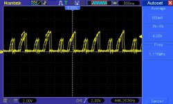
ldkraemer
Veteran Member
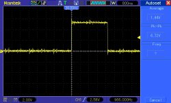
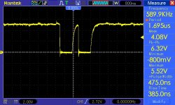
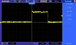
For Pin 3 (A13) on Z21 I'd thing that looks fine. For Pin 10 of Z21, was the DIP Shunt installed?
You shouldn't be seeing a signal such as this. What does Pin 13 (A12) of Z21 look like?
What does A12 & A13 on the Z80 CPU look like?
Larry
You shouldn't be seeing a signal such as this. What does Pin 13 (A12) of Z21 look like?
What does A12 & A13 on the Z80 CPU look like?
Larry