• Please review our updated Terms and Rules here

My project: The SeaOtter Essentials Prototyping Computer

WARNING: Lots of text and images!​

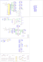
Hello. I've spent some time making changes to the schematic and creating a PCB based off of the new schematic. The SeaOtter Essentials Prototyping Computer V1.2 (design) is here!

Schematic:
Schematic_SO Prototype computer_2023-09-05.png

any part labeled "74LS" is actually a 74ACT series chips. same goes for the PCB layers below!

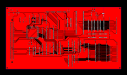
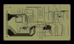
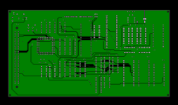
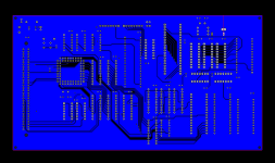
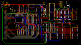
PCB Layers:
PCB_PCB_SO Prototype computer_2_2023-09-04.pngTopLayer.pngInner1.pngInner2.pngBottomLayer.png

I've added Grounding Vias to the PCB design after creating these PCB Layer renders.

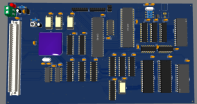
3D Screenshot:
Screenshot (151).png

I've watched a YouTube Video about Traces in a PCB Design and I learned that in digital electronics, Traces that carry data signals need to be as short and as straight forward as possible and need a little space between each trace to avoid crosstalk (The electromagnetic field of a PCB trace affecting other traces). However, the Video said I should worry about cross talk if my design is running at High Frequencies ... the CPU's fastest speed is 12Mhz. However, I didn't hear about the warning for cross talk only being a problem for high frequency. So for a little bit, while designing the PCB. I was trying to make the traces as short and as straight as possible and I stopped the moment I heard the warning for crosstalk only being a problem for high-frequency electronics. However, There still is a need to keep the traces as short as they can be... I've double checked my traces a few times (At least to me) most of the traces look decent in terms of distance. I also learned that traces with too many bends can cause data signal delays, but again I should only worry about that if my design is a High frequency design.

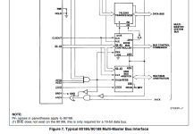
With that mild panic out of the way, I am very proud of my design here. to me, it looks and feels like a motherboard that would be in a home-computer (A computer that has a built-in keyboard and monitor). Speaking of which ... I never was very clear about the kind of computer I am creating here. As already stated, it'll have a built in keyboard and monitor, like a commodore pet or a Sharp MZ-80 computer. I want the motherboard to have everything integrated onto it. The purpose of the expansion slot is to add the next I/O components, which are a Serial Controller and a I/O Controller with an SD Card Interface to be added to the next prototype design. The expansion Slot will also be used for seeing which CPU pins need to be grounded or pulled up to 5v by using Pin Headers and jumper cables or DIP Switches. I know that the CPU should work just fine, but to my understanding having some specific pins on the CPU float can cause some performance hits. Let me know if I obsoletely need to have some pins pulled down to GND or 5v like what's seen in the 80186 Data sheet (Images below) in the replies to this post.
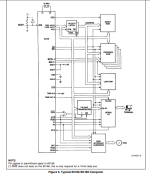
Screenshot 2023-09-05 131013.pngScreenshot 2023-09-05 130942.png

Having A bus transceiver to act as a Buffer for I/O and Memory is directly based off of how the Tandy 1000 did the same thing. The DIR Pins on those transceivers connected to the I/O or Memory Read signal (basically, when that pin is LOW, Data flows from side B to A and when that pin is HIGH, Data flows from side A to B). The output enable is tied to the I/O or Memory Chip Select signals, which is similar to what it is on the Tandy 1000. The biggest Difference is the I/O and Memory Select Signals comes from the CPU directly instead of external chip-select logic.

Going back to the home-computer design for a moment. For the built in monitor, I've found this "Television" on Adafruit's website and while the screen size is only 3 inches long, its a suitable temporary solution until I find something that's similar but bigger.
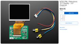
Screenshot 2023-09-05 144637.png

I'm considering adding 8-Bit ISA slots because previous replies told me I could drive ISA Expansion cards due to I/O Read and Write signals, but I might just save that for experimentation later on in this project's life.

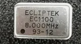
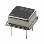
One last thing I have for this post is just a simple question. Is this 8 MHz Crystal from Digikey suitable for proving the x1 and x2 clock input pins for the N80C188-12?

As always, if there is anything I've done wrong or if there is anything I need to fix with either the schematic or PCB design, please let me know in the replies below!
 
Given their low cost and sure-fire operation, I've mostly used XCOs in my designs, unless a crystal is specifically called for.
Its used for the clock generator for the CPU. I have only seen crystals being used for older CPUs, like the 6502, z80 and 8088.
 
Here's the schematic for a Commodore PET that is *kind* of doing what this amounts to; the address signals are buffered and go *everywhere*, IE, to all the onboard stuff *and* the bus connector, while the data bus is only *partially* buffered; the "raw" version goes to the three I/O chips and the ROM... but the buffered version goes to both the onboard RAM and the bus controller. But, again, note that the buffer is indeed *before* the bus connector... and, also, if you look at the RAM schematic there's a buffer there too. In other words, this part of the Commodore PET looks just like the IBM PC, IE, you have onboard devices essentially at the same "buffering level" as a well-designed expansion card on a bus segment where the CPU is the master.

FWIW, this is another general comment about your design: I don't understand why, if you're intending to build extensions for this thing, you've randomly terminated your bus signals onto randomly placed groups of pin rows. What is the point of this? It would make far more sense to bundle these signals into bus connectors that would let you either direct-plug daughter boards or plug in standard IDC dual-row ribbon cables.

I think I suggested this before, but I'll lay it out again: In my humble opinion, in addition to buffering the data lines with a '245 before hitting a bus connector, you should be latching the S0-S2 signals on the same '573s you're putting A16-A19 on, and adding a little bit of logic to generate separate I/O and memory read/write signals as detailed on page 3-5 of this 80188 manual. Doing this will essentially give the signals you need for an ISA-compatible bus subset, and you will kind of need it anyway if you ever want to interface anything to this thing using "discrete" address decoders instead of the U/L/M/P/CS lines. (Which I notice you're running to their own pin headers... even the ones you've already used for onboard peripherals? Not sure what the point of that is.)

Arrange these signals appropriately on a 62+ pin dual row connector and you'd be able to drive simple ISA cards with nothing but a passive backplane board plugged in to convert those pin signals into slots. I would need to read a bit more/scratch my head for a while, but I think you might even be able to run the 80188's INT pins to the some of the interrupt pins on the bus connector (You have four, I would probably suggest mapping those to PC INTs 2, 3, 4, and 7, maybe?) and be able to handle PC adapter boards that require interrupts, like serial controllers. (* obviously you're writing all your own software to do this) You should even be able to drive devices like PC video cards as long as there isn't a memory conflict with your onboard RAM.

Even if you insist against ever putting an ISA slot onto your machine for religious reasons adding the separated R/W signal generation now will make it a lot easier for you to copy existing homebrew designs for your add-on hardware. I mean, if nothing else it is worth noting that you are essentially already out of built-in memory select signals on the 80188; you have a few more PCS signals for I/O mapped hardware, but they'll go fast once you start adding serial ports and mass storage controllers.

Also, I'm sorry, you can't be serious about an 8-layer PCB board. Where are you planning to buy this?
The link for that 80188 Manual no longer works?
 
(Small)PROJECT UPDATES!!!
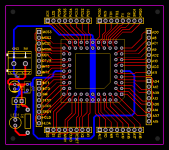
  1. I deigned this Intel 80188 CPU Breakout Board.
    1. PCB_PCB_80188 Breakout Board_2023-08-19.png
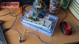
  2. I've Wired up my TMS9918A to my Arduino Uno as I've gathered all of the components for this entire Project. It's wired up to the Arduino for simple testing. At some point, I plan on buying this LCD composite Display to make testing even easier. I followed this YouTube Tutorial and slightly edited the code to work with the Arduino Uno.
    PXL_20231115_144054089.jpg(I'm sorry about the rat's nest made up of these cables.)​

I've been taking a break from this project for a while. so I'll be making small bits of progress here and there as I detail said progress here.
That's it for this post, I'll see you guys in the next one. :)
 
Back
Top