• Please review our updated Terms and Rules here

Need help - repairing a 12-inch monochrome CRT monitor (Daewoo DM-120MWA)

inv

Member
Joined
Feb 26, 2023
Messages
28
Hi all,

I am trying to repair a 12-inch monochrome (green) CRT monitor, Daewoo DM-120MWA, which was made in the 80s for 8-bit computers.

When I got it, it did not work at all. Perhaps somebody might have tried to fix it in the past, I guess. I am a hobbyist without any occasion to learn electronics properly. Actually, I had no background about CRT circuits, so I read some very useful information on CRT repair on the web, but I think I still don't have full understanding. So what I could do so far (see below) was limited and not enough to repair it, or to figure out exactly what part is problematic. (Need help please!)

The problem. When the monitor is turned on, a resistor (R618 in the left hand side of the schematics below) between the power supply and FBT gets very hot quickly, and eventually burns.

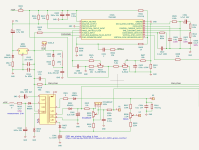
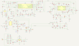
I could not find a schematic or service manual on the web, so I drew part of the circuits on my own (see below). It includes the power supply, horizontal and vertical circuit, but the video/audio parts are not yet drawn. I hope this is enough, because I guess the problem is in the horizontal circuit.

Partial Schematics.
1677590552698.png


The original R618 was 4.7 ohm, 0.5W (9mm long). A replacement R618 luckly lasts for 2 seconds at least, so I could turn on the monitor and quickly perform some measurements (and then turn it off) before it burns.

I meaured the current through R618 with a DMM. It was about 2A. So it was way higher than what R618 can endure.

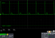
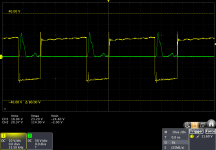
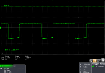
I thought that the reason might be that the horizontal output resistor (Q601 BU806, right?) was controlling the current into FBT correctly. So I measured the voltage of the base and collector of Q601. The waveforms are as follows.


Q601 base waveform
1677591262903.png


Q601 collector waveform

1677591306477.png


I thought that the collector output was problematic. But I could not figure out exactly which part is malfunctioning. Initially, I thought the horizontal output transistor could be the problem. So I replaced Q601 with a new BU608, but the waveforms were the same. So, perhaps Q601 is not why it does not work.

I checked the caps C613 and C614 (I guesses that they are "safety" capacitors... right?). Their values (measured by an DMM after desoldering) look okay.

I also checked the values of caps around the horizontal yoke and FBT: C611, C612, C615, C616, C902. The values look okay. I didn't check other electrolyte caps yet, but at eye inspection, all of them look okay. I also checked D602, D601. Both looked okay.

One thing I noticed was that C901, a cap in the FBT part, was missing on the PCB. I guess C901 was removed by somebody, looking at the remaing solder marks. (R621 and R911 in the schematics are also missing on the PCB, but it is likely that it was originally missing.)

The power supply part works well, I believe. It produces +12V steadily, even when R618 gets very hot.


What could I do from here? Any help and comments will be greatly appreciated!!!


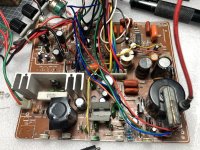
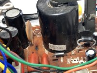
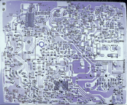
FYI, I attach photos of the PCB.


1677592945507.png

1677592908327.jpeg
 
Last edited:
Basically the H scan stage is drawing too much current, as one possible explanation, but unlikely in this case. The current it consumes depends on the value of the inductances of the flyback transformer and the H yoke coils and the time that the output transistor is turned on.

During active scan time the current climbs at a very high rate at many thousands of amps per second, but , because the horizontal output transistor is only conducting collector current for about 1/2 the active scan time, in the region of 25 to 30uS, it should only rise to a few amps peak at the end of scan. At the end of scan the transistor is switched off, and the stored magnetic fields collapse, and produce half of a sine wave cycle of high voltage oscillation, that you see on the collector recording of the H output transistor Q601. C613 and C614 are the tuning capacitance, which along with the self capacitance, sets the frequency of this resonance. When the collector voltage attempts to fall below zero(gnd) the energy recovery diode D603, often called a damper diode, conducts, clamping the voltage close to zero in the transformer pin 2, which only has a few turns from pin 3, so the collector voltage of Q601 is clamped to near zero. Then this damping kills the high frequency oscillation and linearly scans the left side of the raster. This damped current returns energy back to the supply and lowers the average current consumption, to a value very roughly around 0.8 to 1 amp for this size VDU, that is why it is called energy recovery scanning.

In addition, there is a series diode, D606 and capacitor C616, which charges during scan time to create a B+ boost voltage, the voltage you would measure on pin 1 of the transformer should be higher than the +12V supply (you labelled that -12) at around +18V.

The baseline waveform has two peaks in it just after flyback that should not be there, indicating a possible problem with the damping, however, Q601 is staying into conduction well toward the end of scan.

The most glaringly obvious thing is this; if the average current consumption is say around 1A, the original resistor cannot possibly have been a 4.7 Ohm 0.5W resistor, as the power dissipated in it would be (I^2)R = 4.7W and it would be smoking if it were 0.5W rated, just as it is. Most likely the original part was a 0.47R fusible resistor and the dissipation in it below 1/2 a watt.

Probably everything will come right when you replace it, you could short it out for testing if you don't have a 0.47R resistor on hand.

PS: if C901 is missing it must be replaced, something like a 4.7uF to 10uF 150V to 250V electrolytic as a safe start. You need to test the voltage there and have the cap rated higher than what is there, though probably it is around -40 to -60V. It is for the brightness control circuit, likely for the CRT's g1 grid. If the uF value is not high enough, there could possibly be a turn off after-glow spot that could harm the CRT phosphor, if that happened the uF value could be increased. This capacitor has its positive terminal to ground so watch out for that.

Also, congratulations on taking the initiative to trace out the schematic. Many people appear to give up when they don't have the schematic, but it is right there in front of them on the desk, they just have to take the time and have the patience to copy it out.

I traced out the schematic of this vintage Military VDU, there is no service manual available for it. It was worth it because I was then able to power it. It also contained some very clever circuitry that originated at Tektronix in the 1960's:

 
Last edited:
is it me does or does that large bipolar cap kn front of the flyback look like there is a bunch of gunk at its base? Possible electrolyte leakage?
 
Generally in a 12" vdu one would expect the peak collector voltage of the H output transistor to be in the order of at least 120 to 160V ,and there is only about 96V on the recording, because the incorrect 4.7R resistor is dropping too much voltage, probably at least 4V and the H output stage is under-powered.
 
Thank you so, so much for the comments. It's very helpful, not only for the purpose of fixing the monitor but also for improving my understanding!

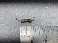
Regarding R618, I think I misread the value as pointed out, given that the expected average current is about 1A. Thanks a lot! The original part (or the part somebody replaced before I got this) has 4 color bands. The last band, which must be silver, looked like gold because it was burnt, I guess. Magically now it looks like silver to my eyes, once I read Hugo's reply ^^;;;


1677670866809.jpeg

It is a 9mm long resistor, so I still guess it is 0.5W. It seems consistent with that the current is roughly expected to be 1A or a bit less.

For further experiments, I removed R618 and connected a DMM with DC current mode, to measure the current when it is shorted. (unfortunately I don't have a 0.47R now). When I turned on the monitor, nothing was shown on the screen. The current through the DMM was 2.4A. It doesn't seem normal. Also, I found that the power supply voltage dropped to about 6.3V, although it was supposed to stay at 12V. I guess it is because 2.4A is beyond the ability of the regulator IC801, an L78S12. (When I had used 4.7 Ohm as R618 mistakenly, the current was about 2A and the PS output was 12V correctly.)

So, I guess there is still some problem in the H scan stage which causes the FBT to draw too much current.

I read the base and collector waveform of the H output transistor again:

Q60_B_C.png

The frequency 15.5kHz looks good, but I wonder whether the turn-on timing is correct, since it might draw too much average current if it remains on too long. From the above readings, the H output transistor is on for about 42us and off for about 0.22us. I found that the horizontal blanking interval (NTSC) is about 11us, and the typical overscan may be about 10% (of the remaining 53us); then a rough estimate of the retrace time is about 16.3us... the above 0.25us is longer, so perhaps the H output transistor turn-on time is not too long... Honestly, I am not sure whether this estimate makes sense. But if it does, perhaps the turn-on timing is not the cause of the high current drawing, I guess. Please correct me if it's not!

Would the yoke or flyback transformer be bad? If so, perhaps it would not be possible to repair this monitor, so I would like to investigate other possibilities first.

If the H output transistor turn-on time is okay, would it be safe to assume that C613 and C614 (the tuning capacitance) work well?

As another possibility, would it make sense to replace the damping diode D603 and/or C615? The collector waveform of the H output transistor still shows additional peaks, even when I short R618. Could it be the reason of the excessively high current?


Once again, thanks a lot for your help and comments!


PS. I added a 10uF 200V electrolyte cap in place of the missing C901.

PS2. The "gunk" VERAULT mentioned: initially I had thought it could be leaks, too, but at a closer visual inspection, it seems like a sort of adhesive which was there originally. Also, it is around large caps in the power supply part, which works well. So I assume it is fine.
 
Last edited:
The H drive waveform timing is normal. Although the transistor is switched on when the beam is still on the left side of the scan, in that time most of the scan current is flowing via the damper diode. The actual collector current does not start to increase greatly until the current is near zero at the center of the screen and it builds with collector current increasing toward the right hand side. Essentially the transistor is turned on for over half the scan time, to make sure there is a smooth transition between the decaying current in the damper diode and the increasing collector current in the transistor. Otherwise there could be a dimple in the scan current if the transistor was turned on later.

With the basically normal looking flyback peak, probably the tuning capacitors on the primary are ok and probably there are no shorted turns in the flyback transformer and probably there is nothing wrong with the the auxiliary circuits that rectify the flyback peak either, except possibly one, the EHT rectifier, that lives in the flyback transformer, but we won't jump to any conclusions yet. It would be worth disconnecting D901, D902 & D903 one at a time, to see if the current drain lowered.

Yes, replace C615 and C616 with new capacitors, it could well be the problem (ps: that is where the +18V should appear on pin 4, when all is normal, I said pin 1 before, typo). Sufficient to check all the diodes on the meter for now.

If C615 & C616 not the problem:

There is something abnormal with the damped current, those two peaks that occur after the flyback on the collector voltage waveform should not be there. The voltage on the transistor's collector is being driven positive by large decaying oscillations on the primary winding, but we are only seeing the positive going tips of two of them (the later ones are snubbed out when the transistor switches on). These oscillations are reverse biasing the the damper diode, so it stops conducting, and the transistor is not conducting either at this time, as it has not been switched on yet.

It raises the possibilities of how that could happen, if C615 & C616 is not the culprit.

The stored magnetic energy in the yoke and flyback transformer is supposed to be returned to the power supply during this interval after flyback, with a linear decay of current via the damper diode D603. During this time though, normally, there are oscillations in the transformer's high voltage (EHT) winding, that are about this frequency, caused by the leakage inductance between the high voltage winding and the primary winding, but these oscillations are not normally seen on the primary winding terminals, because during scan time, the EHT rectifier is reversed biased (it only conducts on the flyback peaks to charge the CRT's anode bulb capacitance). So it does raise the possibility of a failed/leaky EHT rectifier in the flyback transformer, increasing the current consumption and resulting in the primary oscillations appearing. But don't worry, if it turned out to be that, there is a test we could do, it can be fixed by adding an auxiliary one in the EHT wire leading to the CRT. Going against this theory though, is that the flyback peak is still resonable.

Initially at least it would be worth replacing the damper diode D603 as an experiment, you could replace that with a UF5408.

If not that we have to turn our attention to the flyback transformer, EHT rectifier inside it, and H yoke coils and yoke coupling capacitor (that is the large bipolar one). Let me know what happens with the above tests and we move on from there if the problem remains. The next move would be to remove the bipolar capacitor for testing, this also disconnects the H yoke coils and re check the current with the H yoke disconnected like this.
 
Last edited:
Thanks a lot for further explanations and suggestions!

Update: As suggested, I tried the following to figure out why the current through R816 is too high.

1. Tested each of D901, D902 and D903 with a DMM (after desoldering). With each of them removed, the current through R618 was always about 2.5A. It made no difference.

2. Replaced C615 and C616 with brand new caps. This does not make any change (the same high current).

3. Tested each of D603, D606 with a DMM. Looked fine.

4. Removed C612 (yoke coupling capacitor, the large nonpolar one), to see whether the yoke part causes high current. The current measured was about 2.42A. Perhaps it is slightly lower than the previously measured value 2.5A because the horizontal yoke is disconnected. But it is still high, so the yoke is unlikely to be suspicious (right?) I also tested after disconnecting the H yoke connector from the PCB, and obtained the same results, as expected obviously.

In addition, I did the following as an attempt to see whether the secondary parts of the FBT cause the high current drawing.

5. Removed C617 and R619, to disconnect the vertical scan part from the horizontal output transistor. But the current reading was unchanged.

6. Disconnected pins 5, 6, 7 and 8 of the FBT from the PCB. (Because the PCB holes were a bit bigger than the FBT leads, it was enough to remove the solder and clean the area around the pins, leaving FBT in the original position on the PCB. I checked with a DMM that the pins were surely disconnected.) This must remove all the secondary winding loads from the FBT except the high voltage for the CRT anode. (Right?) But the measured current was still 2.42A, i.e., no difference.

I guess #6 implies that the problem which causes high current drawing is unlikely in the secondary side of the FBT (possibly except the high voltage winding). Does it make sense?

I could not yet check what happens if D603 (damper diode) or C612 is replaced, because I do not have new ones. (On a meter both looked fine.) Similarly for D606. Unfortunately, there is no nearby local stores here, so I have to order them online and wait for delivery.

From the above, I guess the problem might be, though I wish it isn't, inside the FBT...

Just in case, to add an additional rectifier to the high voltage wire (I assume it is the red wire to the CRT anode), what kind of rectifying diode do we need? Perhaps it could save time if I order it together with the other parts mentioned above...

Thanks for the help once again, and I will appreciate further comments of course!
 
Last edited:
"Actually, I had no background about CRT circuits, so I read some very useful information on CRT repair on the web, but I think I still don't have full understanding"

For a beginner at this you are doing amazingly well !

All the testing so far suggests the problem is in the fyback transformer. Probably unlikely shorted turns, if that happens due to the very heavy damping normally the flyback peak voltage would be very low on the transistor's collector, though it is possible that there are a small number of turns in the EHT winding that are shorted, but that is not too common, more likely the EHT rectifier has failed.

A BY176 is suitable and there are other options, if we need to, I can explain later how to fit this to the red wire.


What we need to do now is to check the EHT rectifier which lives inside the fylback transformer.

There are a few ways that can yield a result, start with the option you feel the most comfortable with.

1), with the relatively high current drain drain, leave it running for about 30 or 40 seconds. The extra energy as heat; if it is going into the EHT rectifier; will heat it up in the area where the Red wire enters the bulge in the plastic molding of the transformer body, this is where the EHT rectifier is under that long bump down the side of the transformer body where the wire enters. Is that are heating up after it has been running for a while ? Also check if anything else appears to have significantly heated.

2) These EHT rectifiers have relatively large forward voltage drop and a very low reverse leakage (when normal). With the anode wire disconnected, if you test from the anode clip connection on the red wire to the transformer's secondary terminals, generally you should not measure any resistance in either direction with the meter probes, any measured resistance is suspicious. Also check to the primary terminals, sometimes the EHT coil can be terminated to either side, or they might be common.

3) The other method, is to run the set with the anode wire & cap disconnected from the CRT and see if the current drain drops, but, if you do this the Red wire and cap needs to be put well away from the pcb, with the cap put inside a glass jar so that in cannot arc to anything nearby and tape the wire into it around the top so it cannot slip out by accident, or make a thick walled plastic chamber to cover the free end.

4)As an indirect indication: If the EHT rectifier is leaking, there will be no electrical charged stored on the CRT bulb, as it would have bled away quickly after you turn the VDU off. So an indirect test, is to see if there is any stored charge on the CRT's anode connection, if you attempt to discharge the CRT, immediately after turn off, or not.

If it appears that the EHT rectifier is ok, there is a definitive resonance test we can do on the transformer, but it requires a signal generator & scope together. Do you have a typical lab Function generator that can do sine waves up to 100kHz ?

Can you take a scope recording of a signal with the x 10 scope probe tip not connected to anything, bring the probe tip toward the outer round black body (insulation) of the flyback transformer, and it will pick up the signal by weak capacitive coupling and adjust the gain to see the waveform. Have the other channel of the scope locked onto on the H drive waveform you had before shown in yellow . The signal pattern there might yield some useful information.

Also look on the transformer body, is there a multi-digit number. Probably Dalbani Corp have this transformer if we are stuck.
 
Last edited:
I've been busy for a few days, traveling out of town. Today I returned home a couple of hours ago, and did the following:

1. Previously, it was suggested to check whether the current is high when the damper diode D603 is replaced. I don't have a new part yet, so instead, I tested it after switching D603 with D903. (Both are RU2, and I assumed the probability that both went bad would be very small.) It made no changes: the current drain was high.

2. Tested from the anode cap connector (on the red wire) to the secondary and primary terminals. The - lead of the DMM was connected to the anode wire. It showed infinite resistance constantly. When the DMM leads are exchanged, it shows varying values in the 10-150M ohm range for about one second, and then the value becomes infinite quickly.

3. Disconnected the anode cap from the CRT tube and checked the current. No changes. The current drain was still high.

4. Discharged the tube with a screwdriver connected to the metal frame of the tub, immediately after turning off the unit. I could hear a small pop-up sound. Verified multiple times.

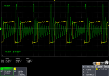
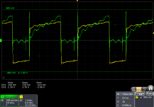
5. Captured an oscilloscope screenshot of the signal picked up by bringing a x10 probe close to the FBT body. Interestingly a very clearly visible waveform was obtained! See CH1 (green) in the screenshot below. CH2 (yellow) is the H output transistor base.

FBT-Q601B.png

I did not checked the heat around the FBT body yet. In fact, after turning on the monitor, the H output transistor Q601 and the regulator IC801 get very hot, so I was a bit worried about that, and always turned off the monitor quickly so far. I guess it would be okay, but perhaps I am small-hearted ^^;;

Unfortunately, the FBT body has little information. No model number is found. The only remaining thing is a label showing "8C04}". (There is another label on the FBT, but all the letters have been completely erased.) I tried to find any related information on the web, but failed. Just in case, the CRT model number is shown in https://oldcrap.org/2020/05/17/daewoo-dm-120m-green-monitor/ .


1677987939446.jpeg
 
Last edited:
Additional update:

After leaving the monitor running for a while, I checked the temperature of the FBT. Unfortunately, I don't have a thermometer that can be used for this, so I used my bare finger. Also, although it was recommended to leave it running for 30-40 minutes, the regulator (IC801) and its big heatsink got very hot (couldn't touch it even momentarily), I did the test for 10 minutes only.

After 10 minutes, I could feel (with my fingers) that the FBT was heated. The temperature was not too high --- I could keep my finger on the FBT body for 10 seconds without worrying about burning at all. Interestingly, the main body part of the FBT (large cylinder) was hotter than "the area where the Red wire enters the bulge in the plastic molding of the transformer body". The temperature difference was definitely sensible, although the gap was not big.

Unfortunately, I don't have a function generator. Though, I guess any information on a "resonance test" for FBT would be still helpful for me. I may try to find somebody from which I can borrow one, or I may try to build a simple alternative using a microcontroller... I never did this, but it could also be fun hopefully ...
 
Hmmm, it is an interesting problem.....That waveform you recorded is never shown in service manuals for VDUs, the only test point, which is not available for seeing it, is the input to the EHT rectifier and it requires a very special high frequency, high voltage probe to see it.

As you can see the two peaks of oscillation that appear on the collector of the output transistor (that should not be there) after flyback, corresponds to the two tips of those EHT winding oscillations, the second peak is chopped in half time wise, when the transistor switches on. No more are visible later after that too, because the transistor gets turned on and it damps them out and their amplitude is falling anyway.

Somehow these EHT winding oscillations are being transformed back into the primary winding, enough to force the damper diode out of conduction on the crests of those peaks, even though, what should be happening is that the collapsing field of the core should drive the damper diode into solid conduction via primary winding current, for the left side of the scan.

So to summarize at this point:

The current consumption is about double normal. The H yoke coils are ok as the problem remains with them disconnected.

It appears there is nothing loading the the flyback transformer output terminals, the auxiliary circuit rectifiers and EHT rectifier disconnected with no effect.

It is abnormal for the flyback transformer to heat up to any significance, that is very suspicious. It is generally a fairly cool running part in these sorts of VDU's. From this we can conclude something is wasting energy as heat.

Normally those oscillations in the EHT winding are never seen on the primary winding. These oscillations come about because when the field in the transformer's core is collapsing, and ringing for half a sine wave cycle (the flyback pulse) as soon as it attempts to take the primary voltage below ground on the second 1/2 cycle, the damper is pushed into hard conduction. This effectively switches a constant voltage across the transformer primary, as you also have when the transistor conducts. If you impress a constant voltage across a transformer primary, it is the same thing as shorting it out, from the alternating current perspective. When you do that, the only inductance which remains in the secondary circuit is leakage inductance. The value of this resonates with the the secondary winding capacitance of the EHT winding, and that determines the frequency of the oscillations there, that you have recorded.

To have some of these oscillations transformed back into the primary winding is uncommon. The only way I could think this could happen is with an additional load on the EHT winding (and its not a defective EHT rectifier), not enough to totally damp the usual resonances too much, but enough to waste some energy and generate some heat. It does not seem obvious how a shorted primary turn could cause this effect. I think, probably, there might be a small number of turns in the EHT winding that are shorted out. Although the turns/volt on the flyback transformers are fairly low , the wires is fairly thin and could act as a resisitive load for the short, and few shorted turns could be enough to do it. Though the only thing troubling me about this notion is that the basic transformer resonances look ok and I would have expected more damping of both the flyback primary peak and the EHT winding oscillations, which both look better than I would expect for a shorted turn scenario.

Regardless of any theories on this, it is easy to blame a flyback transformer for being defective, so before condemning it I think we should do a simple test and find out what the peak current is at the end of scan is.

If you could get a low value resistor, 0.1 Ohms , maybe a 1 or 2W type, or maybe cobble something together from parallel resistors and put this resistor in series with the BU806 (output transistor) emitter & ground and make a scope recording of that, across the resistor, again with the other scope channel sync'd to the H drive, and we will calculate the peak current at the end of scan, just before flyback. That my add some useful information. Do you have an inductance meter ?

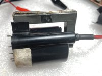
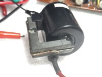
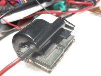
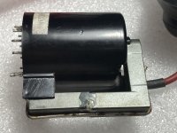
I have one other theory. In the absence of shorted turns one thing which will significantly increase the current drain, increase the peak primary current & heating, would be if the transformer lost inductance for any other reason. One reason could be a problem with the transformer's core. It is very important that the two halves are mated correctly. Looking at a previous photo, it looks like perhaps the glue there has been fractured. Maybe somebody removed the clip and had the core apart, and we cannot see the other mated faces. Check that glue just in case. In any case I can roughly calculate the inductance, if you measure the peak emitter current.
 
Last edited:
.........there is also another thing we can try. Disconnect capacitor C615 on pin 4 and short out the diode D606 feeding pin 1. (two things must be done together, not one at a time)This will ensure that the damped current is returned directly to the supply instead of the boost capacitor C615. Then check the transistor's collector waveform again and the current drain.

This creates a lower energy circuit with no boost voltage. Generally, if you did this to a working VDU the scan width would drop to about 70% of normal.
 
Thanks a lot. I've ordered some parts, including low-value resistors which are needed to do the suggested HOT emitter current test. I'm still waiting for delivery. I expect to get them tomorrow.

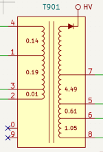
In the meantime, I did a bit more simple investigation on the FBT. First, I wanted to see how the windings are connected to the leads of the FBT, so I measured the resistance between each pair of pins after desoldering FBT completely. (I believe that experts like Hugo would figure it out easily from the surrounding circuit without doing it...) The connection I found was as follows. The numbers are the ohm values between pins.

1678197393529.png

Also, I tested the high-voltage rectifying diode in the FBT. I learned from the web that such a high-voltage diode cannot be tested by the usual DMM diode mode because the forward voltage drop is higher than usual. So I set up a 20V power supply (I don't have a bench power supply so I used a simple boost circuit to get 20V) and connected it to pin 6 and HV of the FBT, with a 3.3 k ohm series resistor, and measured the forward voltage drop. The result is about 17.73V, so I think it is normal. The reverse bias test result was also good (open). I think this tells that the HV rectifying diode in the FBT looks fine.

The following is an updated schematic which includes the FBT windings.


1678196942634.png

One more thing: it was mentioned that the core of the FBT might be bad. It looks okay, but I guess I'm not sure because of my lack of experiences. So I took some photos of it:

1678201090828.jpeg 1678201134814.jpeg 1678201162484.jpeg 1678201184535.jpeg


When I get the parts ordered and perform the suggested tests, I will post an update.

Thanks a lot!
 
Last edited:
The transformer is a standard configuration for a type that uses the boost capacitor. One variation is where the anode of the EHT rectifier connects, sometimes it is to the primary side, it makes little difference. In some cases the short winding between pin 3 & 3 is not there and the damper diode is connected directly to the transistor's collector. In other variants, the Boost winding, boost capacitor and series diode D606 is not used.

Generally, the primary winding (between pin 3 and pin 1) would have an inductance in the range of 200 to 400uH. The total load value in practice comes down to around 100uH when the yoke is connected. Usually the inductance of the yoke H coils is lower than the transformer, so the bulk of the collector and damper diode current during scan goes via the yoke, not the transformer, so obviously it is very abnormal when the transformer, on its own, with the yoke disconnected, is consuming 2.4A.

Have a look at this article I wrote on the PET's VDU, from page 26 on, describes these transformers and how to do a resonance test on them. However, we can estimate the inductance L from the emitter current waveform (You can leave the yoke disconnected). When the transistor is switched on, the timing, from what would be the center of the scan to the R hand side, the current climbs from zero, at a close to linear rate of V/L amps/second, where V is the supply voltage.


Can you measure the cross section of the ferrite core, and the approximate circle that the mounting pins are on and the transformer's height. I think we can find a replacement if it comes to that.
 
Last edited:
Update:

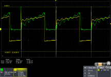
Measured the HOT emitter-ground current as suggested. I used a 0.11 ohm resistor between HOT emitter and ground, and recorded the voltage across the resistor (green below) and the H drive voltage (HOT base, yellow below). The current drain at R618 was the same (~2.4A). The H yoke and all the flyback transformer pins other than 1 and 3 were disconnected.

Q601-E-current-B.png

In the above, the HV anode cap was connected to the tube. When it is disconnected, the waveform is almost identical.

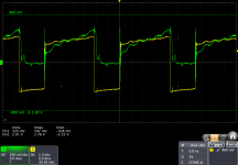
When I connect pins 2 and 4 of the flyback transformer, the result is as follows.

Q601-E-current-B-with-FBT-2-4-connected.png

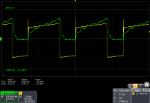
So far, the yoke was connected. After disconnecting the yoke, it changed very little. Just in case, I attach it below.

Q601-E-current-B-with-FBT-2-4-connected-yoke-disconnected.png
 
Last edited:
.........there is also another thing we can try. Disconnect capacitor C615 on pin 4 and short out the diode D606 feeding pin 1. (two things must be done together, not one at a time)This will ensure that the damped current is returned directly to the supply instead of the boost capacitor C615. Then check the transistor's collector waveform again and the current drain.

This creates a lower energy circuit with no boost voltage. Generally, if you did this to a working VDU the scan width would drop to about 70% of normal.

I also tried the above. The HOT base and collector waveforms were as follows. The current drain (at R618) was unchanged (~2.4A).

Q60-B-C-C616-removed-D606-shorted.png
 
Well this is very interesting. As you can see the transistor's emitter current is grossly high and abnormal and has an average value around 300mV/0.11 or about 2.7A agreeing roughly with the 2.4A consumption. At the time the transistor switches on, the collector (and emitter current) should be low as it is damped current in the early phase of the scan, but there is an initial 100 to 200mV/0.11 amp offsett.
I will write again after work today. I will prepare an experiment to replicate the fault in one of my VDU's.

Just to check something you said The H yoke and all the flyback transformer pins other than 1 and 3 were disconnected. In this case there could have been no energy recovery rectifier (damper diode) operating as it was disconnected from pin 2. But, luckily in this case, there is a collector emitter diode inside the BU806 that served the purpose.

It might be worth taking a recording of the emitter resistor again with the primary circuit un-altered, with pins 1,2,3 & 4 connected (except for the disconnected yoke)
 
Last edited:
..............continuing from the above

Ignoring the initial high offset current that should not be there when the transistor switches on (though the emitter current contains the base current contribution), and the superimposed oscillations, the basic sawtooth current is climbing at a rate of (0.4/0.11 )/ 43uS, or about 845666 Amps/sec. Since the power supply is loaded down to 6.3V, the primary winding is behaving as though its basic inductance is 6.3/84566 = 74uH which is much lower than normal.

Loading one winding, such as the EHT winding, decreases (neutralizes some) of the inductance in the other winding (primary) and also more leakage inductance effects are evident. The higher frequency oscillations imposed come from the leakage inductance, All this likely is the result of some turns in the EHT winding being shorted out. I will verify this on one of my VDU's tonight by simulating a shorted turn around the EHT winding, just in case we are missing something. This is also consistent with the transformer heating up. Also, the initial step up in the transistor's emitter current suggests that, as soon as the transistor is switched on, there is immediate transformation of power to some resistive load. Normally, if the load is pure inductance, the current is low initially and rises after time, when a fixed potential is switched across it. Although the load also consists of the tuning capacitors on the primary, these discharge with damper diode conduction. If this is the case, shorted turns, we need to get another transformer.

One thing to check, can you confirm that on your scope trace of the voltage across the emitter resistor is close to zero in the time period where the transistor is switched off ? I was not 100% sure where the DC axis of that green current waveform was ? (just in case the transistor had collector to emitter leakage). One thing that is bothering me though, most of the load current when the transistor is switched on, should still be via the damper diode still, not the transistor, because the field is still reversed in the core and collapsing via damper current and forward conduction of the damper diode, and small reverse collector-emitter voltage on the transistor. Still shorted turns would prevent significant core energy storage. I think you replaced the transistor ? If you have the original transistor, can you re-fit it for a test just to be sure?
 
Last edited:
Just to check something you said The H yoke and all the flyback transformer pins other than 1 and 3 were disconnected. In this case there could have been no energy recovery rectifier (damper diode) operating as it was disconnected from pin 2. But, luckily in this case, there is a collector emitter diode inside the BU806 that served the purpose.

It might be worth taking a recording of the emitter resistor again with the primary circuit un-altered, with pins 1,2,3 & 4 connected (except for the disconnected yoke)

I guess my description might have been a bit unclear. In my latest posting, the first screenshot is obtained when the yoke is disconnected and the FBT pins 1 and 3 are connected (other pins disconnected). The second screenshot is when the yoke is connected and FBT pins 1, 2, 3, 4 are connected (other pins disconnected). The third (last) screenshot is when the yoke is disconnected and FBT pins 1, 2, 3, 4 are connected (other pins disconnected). So the second and third are when the primary circuit is not altered.
 
Last edited:
One thing to check, can you confirm that on your scope trace of the voltage across the emitter resistor is close to zero in the time period where the transistor is switched off ? I was not 100% sure where the DC axis of that green current waveform was ? (just in case the transistor had collector to emitter leakage).

Yes, the green (emitter current) is close to zero when the yellow (base voltage) is low. That is, the vertical midpoint in the waveform plot is actually zero (there is a green pentagonal lable "1" on the left hand side, which indicates the zero level).


I think you replaced the transistor ? If you have the original transistor, can you re-fit it for a test just to be sure?

Yes, I had replaced the H output transistor Q601. All the tests in the previous posts were done with the replaced (new) transistor.

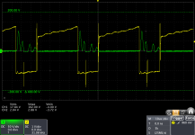
As suggested, I put the original transistor back and did the test again. The following is when FBT pins 1, 2, 3, 4 are connected and the yoke is disconnected. No modification is made in the primary circuit. The anode cap is disconnected.


original-Q601-E-current-B-with-FBT-2-4-connected-yoke-disconnected.png
 
Back
Top