daver2
10k Member
DAve please, lower ram bank is J or I side ? Thanks so much!
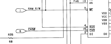
/CAS0 signal going to the 'I' bank of DRAM chips is the lower 16K.
Dave
| VCF West | Aug 01 - 02 2025, | CHM, Mountain View, CA |
| VCF Midwest | Sep 13 - 14 2025, | Schaumburg, IL |
| VCF Montreal | Jan 24 - 25, 2026, | RMC Saint Jean, Montreal, Canada |
| VCF SoCal | Feb 14 - 15, 2026, | Hotel Fera, Orange CA |
| VCF Southwest | May 29 - 31, 2026, | Westin Dallas Fort Worth Airport |
| VCF Southeast | June, 2026 | Atlanta, GA |
DAve please, lower ram bank is J or I side ? Thanks so much!
I tried piggyback also on other video ram and seems to be better but some chars aree wrong...
I have always same result Dave!It might be worth repeating that test again and see if you get the same result.
Ok, can you see something now?Ah sorry, I am thinking backwards...
It was the higher video RAM we replaced last time wasn't it (data bit 7 = inverse video) and you are now piggy-backing the lower video RAM.
It is difficult to see how this would be a problem if the PETTESTER saw the video RAM as working. It must have been working correctly when it performed the video RAM test... So that has to rule it out.
I can't see what I want to see from the video you posted of the manual reset. You need to get a good shot of the PET screen. I can't see the individual characters too well on that video I am afraid.
Dave
Hi Dave, did you take the time to look at how to swap ram? Tks!!Yep, spot on.
There is no problem with the video memory test, but the page 0 and page 1 memory tests are showing some anomalies. I suspect they are transient in nature and, as the PETTESTER continuously tests the memory, eventually it all works.
However, when it then comes to the later tests, because there are some transient RAM issues it causes the code to fail in unpredictable ways.
Please forget the video RAM and concentrate on the main RAM.
There is a way to swap over the two 16K RAM banks. You may have a working upper bank but a problematic lower bank. I will explain how to do that tomorrow.
Dave
")
ok thanks so much!Follow the /CAS0 and /CAS1 signals back from the two banks of RAM. They should go to two (2) resistors.
/CAS0 drives the low 16K bank of RAM.
/CAS1 drives the high 16K bank of RAM.
Desolder one leg of each of the resistors that the /CAS lines go to and swap them over so that each resistor drives the opposite/CAS line that it was originally driving.
Dave
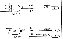
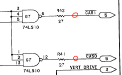
Ah ok sorry!Follow the signals back to schematic number 6. Signals have at least two ends...
Dave
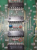
Sorry Dave are these sides?Yes,
Desolder the ends of the resistors you have circled in red in post #173.
Then, wire the desoldered lead of R42 to signal /CAS0.
Then, wire the desoldered lead of R41 to signal /CAS1.
This swaps over the two banks of RAM.
I thought this is what I stated back in post #168?
Dave
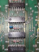
i ma desperate because both R41 sides is wired to G7 PIN 12!! My multimeter sounds beep for every side of this R41 between G7 pinLook at the PCB for R41 to see which end is wired to G7 pin 12, and it is not that one.