• Please review our updated Terms and Rules here

Notes for IBM 5110 keyboard replacement (pin out measurements)

voidstar78

Veteran Member
Joined
May 25, 2021
Messages
691
Location
Texas
I have a full/complete IBM 5110 that works well, but I also have another IBM 5110 that has no keyboard.

They are hard to find keyboards, so I am looking for a way to build a replacement keyboard -- or, better yet: to tether in a cable and use some other device as the keyboard. The connector on this keyboard is a parallel-type interface, not serial.


So, I ordered a Hantek 1008A 8-channel oscilloscope, which isn't super expensive and works adequately for this. But I've just been monitoring 4-pins at a time, instead of a full 8 channels at a time, to keep the cable management less of a mess.


What I've found is this: In the IBM 5110 MIM 2-36 is has a chart of all the scan codes (the IBM 5100 has a similar chart). I tested every key, and each scan code hex corresponds to the parallel voltages used by that key that go across the Z4 keyboard cable on the A1 board.

Using "LEFT ARROW" as an example, it has a normal scan code of 34 hex: 0011 0100

And here are the measured KBD pin values when I pressed the "LEFT ARROW" on my working 5110 system:

B05 KBD_0 0.2v (0)
D06 KBD_1 0.2v (0)
D13 KBD_2 5.0v (1)
B08 KBD_3 5.0v (1)

B09 KBD_4 0.2v (0)
B10 KBD_5 5.0v (1)
B13 KBD_6 0.2v (0)
B12 KBD_7 0.2v (0)

B04 KBD_P 5.0v (1)

i.e. the same "34" sequence described in the MIM as they scan code for this key (and this was observed for all the other keys, they match that chart). However, the trick is that last pin (B04, KBD_P -- parity?), which I don't see documented anywhere. I haven't seen a pattern yet on when it is 0 vs 1 for a given keypress, but I have "measured" what this P-value should be for all the keys.

CMD and SHIFT are key code modifiers, and by themselves don't have a scan code. So you can't determine when CMD or SHIFT (by themselves) has been pressed, or tell the difference between LEFT vs RIGHT shift - on this keyboard, they literally don't cause a KBD STROBE. Best you can do is determine whether CMD or SHIFT were pressed during when some other key was being pressed. Also there is no specific pin for SHIFT or CMD modifies - for most keys it is the KBD4 and KBD7 pins, but for seven keys this is not the case (HOLD, ATTN, LEFT, RIGHT, =, EXECUTE, @). And, my observation was that the value of the "P" pin gets inverted whenever SHIFT or CMD are pressed. For example, for ATTN the KBD_P pin is normally 1, but during CMD-ATTN or SHIFT-ATTN, the KBD_P pin gets inverted to 0.

All "0" bits were measured at around 0.2V, while expected "1" values measured as 5V. So, I'm still not sure why the IBM Z4 keyboard cable has need of 8.5V (other than maybe for the keyboard internal clock that controls signal durations? or maybe it's not really used in this system, and is just a left over interface from some other application).


Next I examined the Power on Reset, Typamatic, Kbd Lockout and Kbd Strobe pins, where the following behavior was observed:

- Power on Reset: this is normally 5v, except press the RESET button is pressed, it went to 0.2V . I'm not sure why the keyboard itself cares when RESET is being pressed (perhaps just that as RESET is being pressed, don't translate any scan codes so that the subsequent startup is in a standard state?). OR, maybe this same interface is just used on other industrial applications that do care when they are being reset.

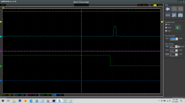
- Typamatic: very few keys on the 5110 keyboard are marked as having typamatic capability (only the arrow keys and the spacebar). This pin is normally 0V (or 0.2V), but when pressing one of these "repeatable" keys, this pin pulses to 5V for ~1ms just after the Keyboard Strobe signal (on the downside, when it goes from 5V down to 0V). Then this pulse doesn't fire again till about another 200ms.

- Keyboard Lockout: nominally 0V, I never saw this signal pulse or go high. I suspect maybe a PALM IOCB can be issued to "lockout" the keyboard, such as perhaps during certain serial or communication processing, to avoid HOLD or DCP being activated during those moments of sending/recieving data. Since I'm not running any such thing, this lockout is probably normal to stay at 0V. Or as mentioned earlier, maybe there are other industrial applications using this same interface (could be what the 8.5V pin is for also, possibly just a carry over from those applications).

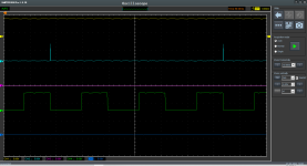
- Keyboard Strobe: Normally this is 5V. Upon pressing any key, this signal goes down to 0V (or 0.2V) for about 58ms then returns to 5V. When pressing a repeat key (like spacebar), this signal stays up for about 48ms, before automatically repeating the sequence (i.e. go back down to 0.2V, send typamatic pulse for 1ms, stay down 58ms, return back up for 48ms, repeat while the spacebar is held down).

All the other pins on the connector are either fixed voltage, ground, or not used.

Hopefully from this is enough information to construct a keyboard replacement. More to come.
 
Last edited:
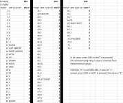
Here are the KBD_P pin values (for the IBM 5110)

5110_kbd_p_values.jpg

NOTE: The IBM 5110 BASIC-only model has some "BLANK" keys, and there are some variations. These "BLANK" keys actually are functional, and it is not a matter of their labels just being worn off (they were released like this). One of them is a PRINT-SCREEN button, the other is some symbol (I forget at the moment). So it is not an error that they are blank, just it was decided as something not-applicable to the BASIC-only model. All of these scan codes apply equally to the APL keyboard (for APL equiped 5110's).


The IBM 5100 is similar Z4 pinout, but uses very different set of scan codes. So the process is the same, but we'd have to discover what the KBD_P values are for its keys. Knowing this process now, theoretically we could resolve the 5100 expected KBD_P values from the extracted 5100 ROS's ? (after some thorough disassembly of the PALM instructions)


Same information below in text format (easier copy/paste), again applies to the IBM 5110 only (well it's possible the 5100 uses the same KBD_P pin values, just I think unlikely -- the KBD_0 to KBD_7 values were all completely different in the 5100 MIM):


INDEX IBM 5110 KEY KBD_P
1 1 0
2 2 0
3 3 0
4 4 0
5 5 1
6 6 1
7 7 0
8 8 1
9 9 0
10 0 1
11 - + 0
12 BLANK 1
13 LEFT ARROW 1
14 RIGHT ARROW 0
15 ATTN 1
16 UP 1
17 DOWN 1
18 HOLD 0
19 CMD 1
20 Q 1
21 W 1
22 E 1
23 R 0
24 T 0
25 Y 1
26 U 0
27 I 1
28 O 0
29 P 1
30 BLANK 0
31 = 1
32 EXECUTE 0
33 NUMPAD_7 1
34 NUMPAD_8 0
35 NUMPAD_9 1
36 NUMPAD_/ 0
37 A 1
38 S 1
39 D 1
40 F 0
41 G 0
42 H 1
43 J 0
44 K 1
45 L 0
46 ( 1
47 ) 0
48 @ 0
49 NUMPAD_4 1
50 NUMPAD_5 0
51 NUMPAD_6 0
52 NUMPAD_* 1
53 LEFT SHIFT 1
54 Z 0
55 X 0
56 C 0
57 V 1
58 B 1
59 N 0
60 M 1
61 ; 0
62 : 1
63 / 1
64 & 0
65 RIGHT SHIFT 1
66 NUMPAD_1 1
67 NUMPAD_2 1
68 NUMPAD_3 0
69 NUMPAD_- 1
70 SPACEBAR 0
71 NUMPAD_0 0
72 NUMPAD_. 1
73 NUMPAD_+ 0
 
Last edited:
Hantek 1008A sample of the keyboard strobe (CH4 green) and typamatic strobe (CH2 cyan) observed on a repeatable key:

5110kbd1.png


Closer view of the typematic strobe during a repeatable-key sequence:

5110kbd3.png
 
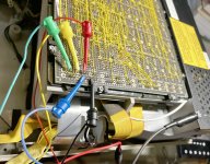
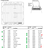
Example of probe connections on the Z4 pins on the backside of the A1 board (well, to me it is the backside - the ROS cards are on the other side).

Note, the hinge is a good ground, and the screw back on the power supply.

IMG_2067A.jpg
 
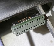
And here is the "project friendly" connector for the keyboard (this is the stock cable that comes with the IBM 5110, fortunately has an "easy to insert cables into" header).

So now it is just a matter of making a device that outputs these parallel voltages on-demand. Think just 10-output channels will do (8x for KBD_0 to KBD_7, then 1x for KBD STROBE, 1x for KBD_P -- I don't think really have to worry about PoR, lockout, or even the repeat features - at least not initially ).


IMG_2070A.jpg


1653694566203.png
 
Last edited:
So now it is just a matter of making a device that outputs these parallel voltages on-demand

Do you know whether the keyboard or the computer is driving the signal lines on the bus? There could be a variety of configurations at work here, including the keyboard raising signal lines to +5V, or the computer pulling the signal lines up to +5V and the keyboard pulling them down, or other permutations.
 
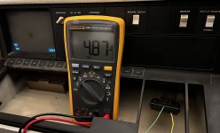
Well, I checked every pin on this keyboard header that tethers over to the Z4 socket on the A1 board...

D08 (green wire) is ground.

B04 (yellow wire) is KBD_P as an example, where it reads 4.87V (system on, underload)

All the other pins also read 4.87V, except:

- the (not used) ones, of course (D02, D04, D05,D10, D12, B02, B03, B06)
- D09 typametic = 0v
- D11 keyboard lockout = 0v
- B11 = 8.33v (under load)

So to type letter A (0x0B for the 5110), turn off/cut the following...

KBD_0_1_2_3 = 0, KBD_5 = 0 (1 0000 1011)
And cut KBD_STROBE all for ~60ms.
(the other KBD_x pins stay 5v as passed-thru from the system)

So you're right, it's not a matter of a device to push power in, but to cut the flow of power already passing-thru?


IMG_2360A.jpg
 
Good questions...

Everyone knows that simple logic signals switch between 0 and 1 by bouncing between one of two DC voltages (not counting fancier forms of signalling). But something has to cause the voltages to move from high to low and from low to high... and it's important to figure out what that mechanism is here in order to work out how to make the keyboard emulator.

One common mechanism works like this. You have a logic line between two parts of the system --- say a keyboard and the rest of the computer. Somewhere along this line, a resistor connects the line to the +5V supply, so absent any other influence, the voltage on the logic line also floats up to +5V. This resistor is called a "pull-up". Now, when the keyboard wants to send data along this logic line, a transistor in an IC somewhere is activated and completes a connection between the signal line and ground, draining the signal line down to +0V. The activated transistor provides a lower-resistance path to ground than the pull-up's path to +5V, so even though the pull-up connection is there, +0V wins. But, when the transistor turns off again, the line floats back up to +5V. The keyboard can use this mechanism to toggle the line between +5V and +0V when it's transmitting data.

A very similar mechanism just inverts the roles of +0V and +5V, so the resistor is a "pull-down" and the transistor pulls the line up to +5V when it activates.

There are other mechanisms too, like push-pull signalling (where pull-ups aren't necessarily needed) and tri-state logic, where devices remove themselves from the bus altogether. These features aren't necessarily mutually exclusive.

Whatever the case, the main thing to know about and avoid is the chance of devices at both ends of the wire trying to move the wire in opposite directions. Say that for your keyboard replacement, the computer had a 10kohm pull-up at its end... but your replacement also puts a 10kohm pull-down on the logic line for some reason. The line will be somewhere around +2.5V, which will confuse everybody. Or, much worse, suppose the logic line is bidirectional and that both ends use push-pull logic. If a bus conflict emerged and both ends tried to drive the line, and if one end connects the line to +5V, while the other end connects the line to ground, now you have a short circuit! And that's a good way to fry something.

You've noticed that the keyboard data lines seem to be floating at +5V, and that's a hint that there's potentially a pull-up resistor somewhere. Can you find it? It could be that the keyboard PCB has a resistor pack that pulls up several of the data lines at once...
 
Last edited:
The Logic section of the 5100 MIM has a few diagrams that might be helpful, and it seems likely that your logic sheets for the 5110 will have similar data.

Page 299 shows a near-schematic of the keyboard. It makes it clear that data lines, parity, and strobe are the keyboard's outputs, while typematic, lockout, and reset are the inputs. Meanwhile, page 276 shows how these lines go into the 5100's Base I/O card.

We had been wondering what the reset line going to the keyboard is used for, and the page 299 diagram clarifies that it resets a handful of flip-flops.

What I still can't work out from those diagrams is how the bus works electrically (that is, the question posed in the last post). There might be pull-ups somewhere (and given that you were measuring the keyboard cable in your photo, they seem more likely to be on the Base I/O card, not the keyboard, my mistake!). Or maybe there aren't any.

The 5100 MIM describes the symbology of its logic diagrams starting at page 256, so perhaps better understanding there would reveal a secret I've missed.
 
The IBM 5110 logic manual is "hidden' at bitsavers in a sub-folder called "diagrams"
I've scanned my own physical copy of the logic manual, so I do have more full sized copies of the individual posters at a higher resolution (and in individual files) - I'm trying to find a place to host them. But the PDF at bitsavers is still good, just all 18 pages together in one file - the keyboard (and tape) are on page 7. (it seems all these logic diagrams are in the MIM also, just slightly different variation) Anyhow, it agrees, the KBD_P and KBD_0 to KBD_7 should be outputs, so how/why are they "floating" at 5V already on the connector side?

I have images of the BaseIO here: (there are a few resistors, but have the impression they aren't for the keyboard - only since I'd expect about 9 or 10 of them in close proximity, not just 5 or 6)
 
Aha, good spot. Bitsavers may still be a good place to host if your images are of higher quality. It's certainly the first place someone would look. It might be worth trying to get in touch with Al?

Those Base I/O card images are really interesting! Keep in mind that pull-ups may come in the form of a resistor pack, which could be what those tall, thin components are. (I don't know for certain.) If you traced continuity all the way from the keyboard connector on the A1 board, through to the connector on the side of the Base I/O card, and finally into one of those (supposed) resistor packs, that would certainly be evidence for the hypothesis. But that sounds like a lot of work!
 
Here is the PCB of the 5110 keyboard, which is loaded with resistor packs (in groups of 10x on left, 8x @ center, and another 10x pack closer to the right side).

I haven't opened the portion below the keys themselves -- I assume that's just contacts of some sort, no PCB content. Unfortunately didn't get a clearer image of the PCB here while it was out, but this is the general gist of the component layout.

IMG_1785A.jpg

EDIT: I'm still trying to wrap my head around it -- if the main system is "supplying" 5v on the keyboard connector pins.... Somehow the ICs on this PCB are re-directing that, so that the system then gets 0v on those lines (as appropriate to whichever key was pressed)? via a different ground than the ground pin of the keyboard connector? (er, maybe not... there is no other explicit cable to the keyboard, but there are 4 mounting bolts that could be grounds).
 
Last edited:
Oh, and regarding the logic manuals on bitsavers: since they are diagram posters, they don't contain a lot of OCR/searchable content. So unfortunately that makes them hard to pop-up on search engines. Maybe just an extra index.html with a table of contents might help on that. I think I did send a message to Al awhile back, I'll gladly submit what I have if given an ftp host to upload to (including to anyone else interested, just PM me). Here's what it would be:

1653935262289.png
 
If the engineers at IBM were anything like their contemporaries, the signals between the keyboard and system unit are "open collector". That is, resistively tied to +5 and pulled low by logic needing to signal. Many MCUs with 5v tolerant I/O can be configured as "open drain", which works fine (the STM32 "blue pill" is one of them).
 
Keep in mind that pull-ups may come in the form of a resistor pack, which could be what those tall, thin components are.

Ah, hadn't considered that. And to clarify to general public: sometimes those tall/thin components are tilted ~45deg, sometimes they are straight up; evidence of these parts being "hand assembled" as opposed to stamped out by machine/factory.
 
I'll also add that when a signal line is unidirectional and open-collector, totem-pole drivers can usually be employed on the signaling end without any problems. Both sides should share the same power supply rails for this to work.

When doing CPLD and FPGA work, "open collector/drain" is often done by manipulating the tri-state control line on the output, which also works. In other words, logical false = high impedance; logical true = totem-pole low. You can also employ totem-pole outputs with isolation diodes in series to the same effect.
 
EDIT: I'm still trying to wrap my head around it -- if the main system is "supplying" 5v on the keyboard connector pins.... Somehow the ICs on this PCB are re-directing that, so that the system then gets 0v on those lines (as appropriate to whichever key was pressed)? via a different ground than the ground pin of the keyboard connector? (er, maybe not... there is no other explicit cable to the keyboard, but there are 4 mounting bolts that could be grounds).

There's no separate ground pin --- it's the same ground. It's just not connected all the time. Here's a model that might help:


That's an interactive toy schematic of a single-key keyboard that makes use of the pull-up mechanism I described. You can see that there's only one shared +5V and one shared ground --- even though they're not shown in the schematic, you can imagine a +5V wire in the keyboard cable and a ground wire in the cable too. Click on the switch symbol (simulating a keyboard key) and watch it go.

When nothing's happening, the keyboard cable data line floats up to +5V because the pull-up resistor, well, pulls its voltage up. This is what @Chuck(G) meant by "resistively tied to +5V".

When you press the pushbutton in the keyboard, it activates the transistor. The activated transistor presents a "low impedance" (that means "very little resistance" in this DC case) path for current in the data line to flow to ground. There is no way that the current trickling into the line through the pull-up can fill the line back up to +5V: it flows out virtually immediately through the transistor. But when you release the key, the transistor shuts, the hole in the bucket is plugged once again, and the voltage can rise once more.

As all this is happening, the computer at the end of the cable can detect the changing voltage in the keyboard data line and react to it.

@Chuck(G) used the term "open collector". This refers to the fact that the part of the logic that's doing the signalling isn't actually putting any energy into the signal line: it's just opening and closing a path where energy supplied externally can flow. If it weren't for the pull-up, there would be no useful signal, since the line would be "empty" already. The "collector" in "open collector" refers to the collector (switched current input) part of the bipolar transistor we've used here; if we were using a FET instead (as you find in CMOS logic, which is what you'll find in any microcontroller that you are likely to buy), the equivalent transistor part is called the "drain", so that's why Chuck also said "open drain".

As for the "open" part, I dunno, it's just, like, open, man... to whatever goes into it I guess... far out...
 
And --- as before, this open-collector method is only one kind of signalling scheme that you might find in use in an application like this. However, Chuck's familiarity with these things and your measurement of nearly +5V on the data lines suggest that this might really be what's going on.

Can't hurt to uncover more evidence (as long as you handle all of those components carefully --- beware ESD!), but as you've experienced with our power supply adventure, you know how I like to be cautious.

It is worth saying that while I am verbose, Chuck is surely much wiser in these matters than me!
 
Wow, thanks for the interactive model, that's really neat (the little yellow dots are animated when the key is pressed down, that's cute).

Per the MIM there are a couple other things, just to have them noted:

(1) when the key is pressed down, the scan code goes into a buffer (and it mentions using a "scan counter"). i.e. "The key data, which includes an odd parity check bit, remains in the character register until the key is released." I did think the P was parity and I recall that being related to just the count of the number of bits -- and that's consistent with the measurements I made earlier (scan codes with even number of bits is KBD_P=0, otherwise KBD_P=1; which also explains why pressing CMD or SHIFT inverts that, since those impact just one bit).

(2) There is also the KBD_STROBE that triggers "from the keyboard latch to the data select register and requests a program level 3 interrupt." which then "a level 3 microprogram converts the key code to the 5110 internal code through a translation table located in Common and Language ROS (F2)". This should basically be handled like a key-press, just that it has a timed delay to start and a duration.


Ok, so replicating this keyboard input won't be trivial. My tentative plan of attack is this:


An Arduino Nano (ATmega328P based) to be able to hookup a modern/normal USB keyboard, listen to keys, translate into appropriate 5110 scan code. I think I have a handle on how to do all that.

Then communicate that scan code over to another device configured in this "open drain" pin configuration. I'll try either:
‎NUCLEO-L432KC‎
or
STM32F103C6T6 (blue pill, as suggested)

Hopefully between one of those, the output pins can handle the 5v (and I think I need 10-outputs; 8 data, 1 parity, 1 strobe -- I might not get the repeat feature working, but I think there are 12-14 digital pins available anyway). And I can feed all that with the 5V pin already in the 5110 kbd header.

And I can rig up a "5v source system" to test things out before connecting to the real system.

Also, I think I can attach a SD-reader to the Arduino Nano. So I was thinking of a sort of "player piano mode" where it reads a file from the SD-card and issues those commands as-if typing them into the 5110 (like the scripted inputs used in the VEMU5110 emulator). But I'm not sure how extensive the existing API software library for doing all that is, or how much SRAM it'll take (extra code is needed to parse the files on the SD, and translate ASCII over into 5110 kbd scan codes).


I'm not sure if this could be plugged in-line with an existing keyboard. i.e. electrically I'm not sure is basically two keyboards could be connected at the same time? i.e. this will probably a unique 1-off build, since I'm not sure folks who have functional keyboards already will make use of something like this.


Also, there were some notes about "simulating" this open-drain effect on the Arduino, but I'm not sure if it has enough pins to do both jobs - having just one device would help simplify things. So alternatively, I'll see how hard USB-keyboard input on one of the STM32 devices might be (it might have enough extra pins to do it).
 
Last edited:
Back
Top