• Please review our updated Terms and Rules here

NS32000 Series Family Thread (porting TDS to a NS32016 user wire-wrap board)

migry

Member
Joined
Jun 14, 2020
Messages
38
Location
Cambridge, UK
I hope it's OK to start a new thread. I previously posted to a more specific NS32016 board (PD32) in another thread.

I'm not exactly sure why, but my interest in the NS32000 family has been re-awakened recently. FYI, I worked for Nat Semi from 1982 to 1986 (in the UK), but spent the whole of 1985 at the headquarters in Silicon Valley. I worked on the test systems and did some characterisation work on the NS32016. Just for the record, at that time, the NS32016 (and family) were tested on the Genrad GR16 VLSI tester. I heard a rumour that Atari has considered using the NS32016 in the Atari ST. I am still gutted to this day that they chose the 68000!

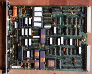
At the time I got my hands on a small number of parts. In 1986/7? I built a wire wrap board for a very basic NS32016 system, and wrote a simple boot loader. Ironically I used an Atari ST and wrote an asembler in Pascal. Otherwise I didn't move the project forward. Fast forward to 2019 when I got the old board out. I generated schematics in Kicad and disassembled the boot loader, only to find a bug caused by my old assembler. A second bug limited the amount of code to be loaded over the serial link (INS16450) to less than 255 bytes. I wrote a new assembler in Perl and played with a 2nd stage boot loader. I'm not sure but I think that the hardware was a little flaky, so again I didn't make much progress.

I recently found the PD32 thread on this forum and it may have kick started some renewed interest. I also started playing with various tools recently found on the internet. I was able to get the DSI compilation tools to run and the code could be run on the NS32016 emulator. Now I have always wanted my board to run the TDS (Tiny Development System) software, but I have never found a ROM dump. I would have had to disassemble it, in order to change the UART code from the INS8251 to the INS8250/INS16450. So I tried to assemble the source code to TDS. This worked but I couldn't figure out how to link to a ROM binary. So I merged all 10 modules together, and started to modify my own Perl assembler to add support for the Genix assembler directives. I also modified the output listing format to be the same as the Definicon/Genix assembler. There were a number of issues to solve, such as module name clashes, but I was finally able to generate binaries and blow 27128 EPROMs with the code.

I then took me about 10 iterations until I had something working. There were a mixture of hardware and software "bugs" to fix. My board had 2 x 6264 RAMs (8k x 8) and 2 x 27128 EPROMS (16k x 8). The first code crashed. I used the 16 channel logic analyser on my scope to follow the code (using the AD bus for address and data, and CS for a scope channel) and found it crashed after a jump into high memory. The FF's were unexpected, but then I realised that I had tied off the upper ROM address bit so that only the first half of each EPROM could be accessed. Brought about due to using as LS139 to decode each 16k bank of memory (but the EPROM was 32k). So I ORed two of the LS139 outputs and wired up A14 to the EPROMs. Now the code ran and printed a sort of welcome banner. I forget everything I had to debug, but I had to write link tables for traps and module tables. I also found that "main" needed it's own module pointed to by SB otherwise on return from a SVC call, SB was loaded with random data!

I added circuitry to single step using a Arduino Mega2560 as a bus master. This has been quite interesting, particularly when executing the more complicated instructions, which do things in a slightly different order to that documented. This has been vital in tracking down the various bugs for each of the ten ROM releases.

Anyway after 30 odd years I can finally run TDS on my own hardware. I was able to type in the program from the user manual and get it to assemble, but the system crashed when trying to run the code and of course I lost all the source code. I intend to add a Flash EEPROM to use as "tape" storage, as a solution to losing source code on crashes.

More information here.

I'll post updated pictures to twitter and give a pointer.
 
Folklore suggest the the N32 series chips were buggy and flakey, and that was one consideration that vendors used to not select them. Do you (or anyone) know anything about that? How it was manifest? Was it a batch error for some specific chips, was it systemic, etc.? Did the chip ever get sorted out or just run over by history.
 
I think bugs were present only on the initial 16032/32016 chips, which were very late (I started talking about them to the NS guys in 1979).

I think that the later chips, as used in laser printers (NS32CG16), etc. were pretty solid.
 
I regularly search for "NS32016" just to see if any new information has appeared. I read somewhere a similar statement regarding reliability, but I have no idea where the source of that "rumour" came from.

I did download a very useful errata document. My NS32016 CPUs are 1985 vintage rev "M". I was a little shocked at the length of the errata, but perhaps for such a complicated CPU we shouldn't be too surprised. Some issues sound like they stem from timing issues inside the chip. Nowadays there are very powerful STA (Static Timing Analysis) tools which can help find these issues well before tape-ship/tape-out.

I do recall a rumour (1985) that 10MHz yield wasn't as high as would have been liked, and that it might have resulted from critical timing between the NS32201 TCU and the NS32016 CPU. At that time the CPU worked on 2 phase clocks (I worked on similar architecture chips at a different company a few years later) which introduce these critical internal timings. I've always wondered if skewing the various phi1/phi2 clock edges might eek a little more speed out of the CPU. Nowadays similar designs all use D-type flip flops clocked from a single rising edge (sometimes the neg-edge is also used but the quantity of these flops is a small percentage - at least on the products I recently worked on).
 
Just stumbled across this thread. Since you worked for NS in the UK in the early/mid '80s, did you have any interactions with people at Whitechapel Computer Works?

You might be able to shake hands with the Rev. N NS32016 in our WCW MG-1 if you visit port 31132 of mg-1.uk in your web browser (not linking to keep the spiders away). It all depends on whether the RasPi I'm using as a wifi bridge feels like talking to the home router. (Often it does not.) Even then, response time may be even slower than you'd expect, since right now I'm running disk I/O intensive jobs in order to help debug the MFM drive emulator we are using :)
 
Just stumbled across this thread. Since you worked for NS in the UK in the early/mid '80s, did you have any interactions with people at Whitechapel Computer Works?

No. I had no contact with any customers because my job role was "test".

BTW I did try to connect, but couldn't figure out the URL. There are pictures on Udo's website, and I tried the URL captured in the image, but still no luck.
 
So I have been busy on NS32016 related projects.

I have created a NS32016 CPU board, which implements my single-in-line connector for easy use in plug-in breadboards. I also generated a mk2 version of my RAM card, and I also made a backplane (since it was getting painful using wire links on a breadboard!). Pictures can be seen on my twitter account "migry_tech". I tried uploading a JPG but it was too big :( I will try to find a way to resize and post later.

I am now playing around with the NS32016 GCC cross compiler. I will be posting some questions in the near future!

Anyway over the weekend I debugged the CPU board. I was able to load some C code compiled with GCC into the SRAM and execute it on the NS32016.

Just some background. Over the past 6 months I have been playing with the MC68000, since I have fond memories from my Atari ST ownership days. My interest was kicked off by the "Katy" project. I built up my own version on breadboards, but found the wiring up tedious. So I used Kicad in anger for the first time and made a single-in-line memory board PCB. I later followed this up with a MC68000 DIL and then a PLCC single-in-line board. I used breadboards to hold the boards and wired between them. So I have a CPU card and a memory card and also my own FPGA card (on which I have implemented video). I use an Arduino MEGA2560 as the bus master and it uses DMA (slowly) to load the binary into the RAM (there is no ROM). Using the Arduino I can run or single step, load memory from SD, and peek and poke. During tracing I disassemble the executed code. This allows me to see where I am in the C source.

So the NS32016 board works in the same way. I implemented tristatability of the bus and the Arduino can put the CPU into HOLD, which tristates the address latches and databus buffers. The upper address is tristated by the CPU. I use a GAL to tristate ADS, HBE, RD and WR. The other GAL handles single stepping. Ironically I made a error soldering in two adjacent SMT resistors. I soldered them left/right instead of up/down. Once corrected I still had problems. I had wired RWEN to +5V instead of GND! Easily fixed however thanks to using a resistor rather than a hard tie. The bug tristated RD and WR, making me realise I could have eliminated the 2nd GAL (which essentially tristates a few signals from the edge connector bus).

Today I hacked together a INS16450 UART board, which I am just about to test. I hope to then get my version of TDS to work on this new setup. It is already running on my wire wrap board.

More later...
 
No. I had no contact with any customers because my job role was "test".

I mean this question quite sincerely and not as a dig: given that the NS32016 had a reputation for bugs, at least in early revisions, did your test role have much to do with finding those errata or identifying workarounds for them?

BTW I did try to connect, but couldn't figure out the URL. There are pictures on Udo's website, and I tried the URL captured in the image, but still no luck.

I'm feeling bolder now, and the RasPi seems to be working okay: visit http://mg-1.uk:31132/
 
I mean this question quite sincerely and not as a dig: given that the NS32016 had a reputation for bugs, at least in early revisions, did your test role have much to do with finding those errata or identifying workarounds for them?

Simple answer - no! I was new to Nat Semi, in fact it was my first job. I got to spend 6 months at the headquarters in Santa Clara (Silicon Valley), which was quite an experience, both good and bad. I worked on the VLSI testers, the machines that test each IC to confirm that it is not faulty, that is not the same as the validation function, which checks that the device operates against it specification. What the tester is able to do however, is to measure the AC parameters to confirm that the AC specifications on the datasheet are met. This includes FMAX. I recall that the test software first tested each CPU at 10MHz, then if any "patterns" failed, changed the timings to 6MHz (I don't recall) and re-ran all test patterns (known as speed binning). I was not privy to any detailed test issues, but I sort of recall that 10MHz yield was a major issue and had something to do with the timings of both the TCU and CPU.

I think that the 32016 family was designed in Israel (but I was unaware of that at the time). The testing was certainly done in Santa Clara. As to where the silicon validation was done, I have no idea. Nevertheless the fact that even at that time the 32016 CPU rev was N, speaks to the number of silicon problems that must have been found. Also remember at that time CAD tools were primitive (if they existed at all) as compared with todays design flow. I am guessing that most if not all of the design must have been done by hand, including layout (no auto-routers back then AFAIK).

I'm feeling bolder now, and the RasPi seems to be working okay: visit http://mg-1.uk:31132/

Thanks. This site is working.
 
Just a heads up to anyone who might be looking for either some NS32000 family ICs or a complete system, on Ebay UK (might actually be Ebay De) there is a German seller who has listed "National Seminconductor NS32032E, mit 32081, 32082, 32201, 32202, 10 Mhz, 32 Bit"

ns32032-Ebay.JPG

It's a buy it now price of around $100 (postage extra). Seems a reasonable price to me. FWIW the CPU is the NS32032E-10 rev H. There's a TCU, FPU, MMU and ICU all rated at 10MHz.

Some research might show whether it is a known board on Udo's excellent web site.

Of course the other seller who lists NS32000 series parts on Ebay UK is a company called Little-Diode, whose selection of old devices is impressive, however whose prices are sky high, often 10x the normal going rate (as compared to other sellers).

I also recently found that some of the "newer" devices such as the NS32FX16V can be found on the UTSource website at reasonable cost. I've never ordered from here, but a friend has and suggested to me that he trusts this site more than Ebay or AliExpress (having ordered via this site).
 
I got fake HD63C09 (blacktopped), MC6820 and 2n5109 from UtSource, same quality as Ebay or Aliexpress :(
It isn't a reliable supplier (like all Chinese) and it is very difficult to get a refund, you need to send the products back to China and it costs a fortune from France.
 
Regarding viability of the NS32xxx chips, Sequent Computer Systems made their first SMP machines using these (while they waited for Intel to get the 80386 working). I don't know the total number of customers or machines, but they sold them for several years. NASA Ames had one. Many years later Sequent donated their last one to the Smithsonian.
 
It's been a while since I last posted. I have been working on some NS32016 software, debugging it using the available emulator (plus my own additions). Soon I would like to try running the software on my hardware which is a set of boards: CPU (NS32016+NS32201); memory (4M bytes organised as x 16); UART (INS16450), with code loaded using DMA controlled by a Arduino MEGA. The board currently runs my hacked version of TDS.

A short while ago (couple of months?) I installed a NS32202 ICU and updated TDS to do simple initialisation to display a pattern of 0x55 on a LED bar. During this time I discovered a wiring mistake for the ICU databus and added hack wires to fix. I updated the TDS ICU init code to put the device into 32 bit counter mode and I saw a square wave on COUT.

I want to debug interrupts in order to port my big project code. So a few days ago I fired up the "system". I added a LED on the COUT pin. At some point I noticed that the LED bar was not lit up. I also had problems with the sytem doing random crashes, possibly after it had been on for some time. Note that I currently run the NS32016D-10 (rev N) at 4MHz, and I was using a 6MHz TCU (which got very hot). I swapped this for a 10MHz TCU part and added a small copper heatsink. The system now seems reliable, although the TCU copper heatsink gets too hot to touch. FWIW the CPU is hot and the ICU is warm. I recall reading something about the NS32016 having a minimum operating speed. No idea if this is related to my problems. The ICU is still not displaying the pattern on the LEDs, so I decided to investigate. What a rabbit hole!

I use a GAL16V8 to decode A23, A22 and A21 to decode 0b111 and connect this to the ICU because it needs to be addressable at 0xFFFE00. The UART decodes A23, A22 and A21 using the 3 chip selects to decode 0b110 putting it at address 0xC00000.

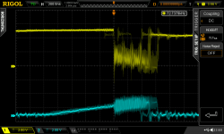
When I scoped the ICU CS (chip select) I saw some horrid noise. What puzzled me is that I was sitting in a loop (in TDS) waiting for a character to become available on the serial input (connect via a serial to USB adapter and using TeraTerm for I/O at 19200 baud). The ICU CS should have been inactive.

ICU CS and A21 noise.png

I sort of figured out what was going on. The UART status register was being accessed in a wait loop. Address bit A21 (bottom trace) was doing something strange and the top address bits 0b110 with a strange A21 were being decoded by the GAL as 0x111 and so generating the horrid ICU CS. I still don't really know why there is the horrible oscillation.

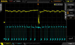
I found that poking around with my fingers and touching the upper address pins, I could get ICU CS to stay high. WTF!!! I scoped the upper address bits and they were all suspicious as if they were being tristated and were starting to float high. However I use DMA for loading the RAM and I checked that the "HOLD" control from the Arduino was solidly high. Now I do not have a MMU installed so DS/FLT is a data strobe output and not a float bus input. So I as far as I am concerned, and checking the databook, A16 to A23 should always drive. Just for a check I scoped ICU CS and FLT.

ICU CS and FLT.png

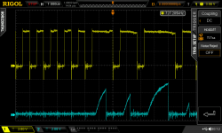
The traces were a little suspicious. The blips on A21 (not shown) corresponded to the gaps where FLT is high. But it is clearly a data strobe output and can't possibly be floating the upper address bus. So I experimented with adding a 10k resistor to A21 and either GND or VCC. This seemed to confirm that A21 was being tristated. WTF(2)! The next scope trace shows TSO (more or less the same gaps as FLT) against A21 with a 10k pull-up to VCC.

ICU CS with pullup and TSO.png

So what on earth is going on? I know that A16 to A23 can be tristated, but if there is no MMU and HOLD is inactive, I would have expected these pins to always drive. Clearly this is not happening.

What is strange is that a month or so ago, the ICU appeared to be working correctly. The only thing I recall doing was to wire a spare LED in the LED bar via a resistor to COUT, such that if a programmed a large divider value I could see it pulsing slowing and use this as a test interrupt.

Also FYI, when I single step the intialisation code, I see the 3 writes to the ICU which configure the 8 bit I/O port and I see the LEDs display 0x55, but as soon as I step further and write to the ICU_MCTL register to stop the counter, the LEDs go off and the I/O port seems to go back to tristate. Although the databook is not clear, this register seems unrelated. However after the next few writes I do see a 1MHz waveform on COUT. If I go into "run" mode, and leave the pull-up in place to fix A23(?), there is no waveform. If I edit the ICU registers in TDS (using the cmb command) then I do not see the LEDs lighting. I suspect I still am getting ICU CS when it should be inactive and this is corrupting the ICU registers.

Any ideas why the upper address bus is going tristate when the CPU is not accessing the bus?
 
I don't know the NS32000 CPUs at all, but I'm not sure you can make any assumptions about the state of address lines in between the various control signals going active. There's typically a guaranteed address setup time where they will be valid before the RD/WR, but otherwise I don't think you can assume anything. Are you saying that your GAL activates a peripheral chip select without getting an actual RD/WR or least IORQ signal from the CPU?
 
I don't know the NS32000 CPUs at all, but I'm not sure you can make any assumptions about the state of address lines in between the various control signals going active. There's typically a guaranteed address setup time where they will be valid before the RD/WR, but otherwise I don't think you can assume anything. Are you saying that your GAL activates a peripheral chip select without getting an actual RD/WR or least IORQ signal from the CPU?
I had the same thought. According to pages 17-18 in this PDF there is an address strobe line /ADS which goes low to indicate a valid address. I imagine that would need to tie into the chip select logic. http://www.cpu-ns32k.net/files/NS32C032.pdf
 
I had the same thought. According to pages 17-18 in this PDF there is an address strobe line /ADS which goes low to indicate a valid address. I imagine that would need to tie into the chip select logic. http://www.cpu-ns32k.net/files/NS32C032.pdf

Ah, yes, enlightening. So it's actually a multiplexed data/address bus and one can *only* assume the address is valid while /ADS is active.
 
Thank you for the replies. I will answer the items raised shortly.

Posting to this thread made me think about the problem, just like explaining a bug to a colleague at work. You often see the reason for the bug before your colleague does!

I now understand the problem with the ICU not working, however the apparent tristate behaviour of the upper address bits is still puzzling.

For non NS32000 family people, I should have explained that the ICU is the NS32000 family "Interrupt Control Unit". The NS32000 CPU family have an INT (active low interrupt pin) which can be used in a simple way, or as part of a vectored interrupt feature (sort of like the MC68000). The ICU supports the vectored interrupt feature and has 8 (or 16) interrupt inputs, either edge triggered or level sensitive. It can be wired to the CPU in either 8 bit mode or 16 bit mode. In 8 bit mode 8 pins are freed up and can be used as an 8 pin general purpose I/O port. This is what I have done and these 8 I/O pins connect to a LED bar. The ICU also includes some timers, which can be configured as 2 16 bit timers or combined as a single 32 bit timer (this is the mode I am currently using).

I am puzzled as to why National gave the user two options as I don't see a big advantage of the 16 bit interface over the 8 bit. OK some of the counter registers in the ICU are 16 bit so can be accessed a little easier/faster. I am also puzzled why they didn't take advantage of the AD15-0 (combined address/data) bus which would have saved the 5 address inputs. As compared to other timer/interrupt ICs, I always found this device a little confusing, perhaps not helped by the datasheet.

The mis-behaviour of the ICU and non lighting of the LEDs was caused by a software bug. My bad! In the very original ICU code I simply wrote to the I/O port. The default/reset mode of the chip is 8 bit.

Code:
                                  9784  ;
                                  9785  ;  I C U   R E G.
                                  9786  ;
                                  9787  ICUBASE:  .EQU   H'FFFE00        ; ICU REGISTER  0 ADDRESS
                                  9788  ICU_MCTL: .EQU   ICUBASE+16*2    ; ICU REG 16
                                  9789  ICU_PDAT: .EQU   ICUBASE+19*2    ; ICU REG 19
                                  9790  ICU_IPS:  .EQU   ICUBASE+20*2    ; ICU REG 20
                                  9791  ICU_PDIR: .EQU   ICUBASE+21*2    ; ICU REG 21
                                  9792  ICU_CCTL: .EQU   ICUBASE+22*2    ; ICU REG 22
                                  9793  ICU_LCSV: .EQU   ICUBASE+24*2    ; ICU REG 24
                                  9794  ICU_HCSV: .EQU   ICUBASE+26*2    ; ICU REG 26
                                  9795  ICU_LCCV: .EQU   ICUBASE+28*2    ; ICU REG 28
                                  9796  ICU_HCCV: .EQU   ICUBASE+30*2    ; ICU REG 30

...

                                 9884
                                  9885  ;;;;;;;;;;;
                                  9886  ; NS32202 ;
                                  9887  ;;;;;;;;;;;
00004252 PC                       9888          .ALIGN 2
                                  9889  INITICU:
00004254 PC 54a500c0fffe28        9890          MOVB    0x00,@ICU_IPS               ; ports are I/O
0000425b PC 54a500c0fffe2a        9891          MOVB    0x00,@ICU_PDIR              ; ports are all output
00004262 PC 54a555c0fffe26        9892          MOVB    0x55,@ICU_PDAT              ; initial pattern

This is what I recall working.


Nevertheless in investigating this problem I discovered the strange upper address bus anomoly and the horrid unexpected ICU chip select.

Poster @durgadas311 is correct when mentioning the importance of /RD and /WR. I forgot to explain that at the same time I saw the horrid ICU CS, both /WR and /RD were high/inative. So there should have been NO access of the ICU regardless of the chip select to the ICU. I (wrongly) assumed that this was causing the ICU to misbehave when it was a simple PEBCAK software bug. Nevertheless I don't feel comfortable having that waveform of chip select in my system.

I later added more code to configure the 32 bit timer. In doing so I wrote a '1' to a bit in the register which enables 16 bit databus mode! Further writes are interpreted differently as a consequence and the ICU registers are essentially corrupted. Simply changing this bit to zero resulted in the LED bar lighting and a nice squarewave being seen on the COUT pin.

Code:
00004269 PC 54a502c0fffe20        9893          MOVB    0x03,@ICU_MCTL              ; 8 BITS INTERFACE,COUT OUTPUT,SQUARE WAVE,COUNTER OUTPUT TO PIN COUT

The MOVB value 0x03 should be 0x02 for 8 bit databus mode. 0x03 selects 16 bit databus mode.

As to /ADS. This signal is used to latch the address from the multiplexed AD15-0 pins into (usually) 74LS373 8 bit latches. It is generated by the TCU and indicates the start of any read or write cycle. It doesn't need to go into any chip select logic. In this case simply decoding the upper address pins to generate one or more chip selects is perfectly valid, and in fact I see this was done in a National application note for the NS32CG16. Any decoded chip enable also needs the /RD or /WR to be active in order to enable the selected chip/memory.

As to the comment "I don't know the NS32000 CPUs at all, but I'm not sure you can make any assumptions about the state of address lines in between the various control signals going active" this information is usually well documented in any CPU datasheet, and the behaviour of all pins, as to their input or output state is very well documented. This is particularly critical of any CPU databus, which by it's use switches between input/output/tristate/inactive modes. Since the NS32000 CPUs support various pins being tristated (using the /HOLD input) the behaviour of all affected pins is well documented. There is an added complication for the NS32016 if used with the NS32082 MMU, where the MMU used the CPUs /FLT input to tristate the CPU address in order to put its own translated address onto the main address bus (A24-A16 and AD15-0). In the case of no MMU the /FLT pin is actually an output called /DS (data strobe) and goes low whenever there is a read or write, sort of like the /TSO output from the TCU.

According to my interpretation of the datasheet, the upper address pins A23-A16 can be tristated, either when /HOLD goes low, or when the CPU is used with a MMU and the MMU forces /FLT low.

I checked with the scope, and I am seeing the suspicious rising level on the A23-A16 pins when the CPU status from ST3-0 is '0000', which according to the datasheet "0000 - idle CPU inactive on Bus". Hmmm, which bus? AD0-15 bus? AD23-16 bus?

Wow who would have thought? Perhaps in the idle status cycle ('0000') all data and address pins are really tristated? If this is really true then it isn't clearly documented in the datasheet. I have never seen it mentioned in any NS32000 documenation.

So poster @durgadas311 IS 100% correct with his statement "I'm not sure you can make any assumptions about the state of address lines in between the various control signals going active". I would have put money on the upper address bits always driving, even with the bus idle. I had assumed that the upper address bits would always drive (even during idle cycles) as this is what I have observed on other micros. Wow! Colour me embarrased!

I think that this now explains the upper address bit behaviour, and I need to consider adding pull-ups/downs, as a floating address bus is never a good thing.

Thank you for helping me think more clearly! :thumbsup:
 
I noted the reply from @bakemono , which caused me to look at the NS32C032 datasheet. The PDF was searchable and I searched for idle and found some interesting references I hadn't previously noted in my paper NS32016 databook. So I then moved to the more applicable NS32C016 PDF which was also searchable.

It's still not 100% clear to me, but there are mention of idle states, both in reference to going into tristate after asserting /HOLD (this idle seems to be called Ti) and also as a result of the MMU asserting /FLT (this idle seems to be called Tf). I'm not sure if Ti and Tf are the same thing. Again I assume(!) that these idle states are the same as when I saw the ST3-0 pins as "0000" on the scope.

I now have found in the paper databook, figure 4.6 (figure 4.7 in the PDF) "Floating by /HOLD Timing (CPU initially idle)" where it shows a couple of Ti states, both AD0-15 and A16-23 are clearly shown as "FLOATING".

This does appear to confirm that when the CPU is in the idle state, the upper address bits are tristated. This really surprises me!

[NOTE: I am still under moderation. Yesterdays posting was posted immediately, todays earlier reply told me that it needed to be moderated, so not clear whether this reply will appear before today's earlier posting, which will help this posting make more sense.]
 
Back
Top