• Please review our updated Terms and Rules here

Pattern Recognition in PET Repairs.

Hugo Holden

Veteran Member
Joined
Dec 23, 2015
Messages
4,773
Location
Australia
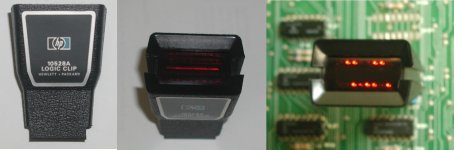
The recent post by Scottish Colin with the IR photos of the PET board and the work done by Nivag on logic signatures and the scope photos of the 20 or so scope recording I made of the DRAM support circuitry in the PET got me thinking. About all the possible ways we could build up a data base on the PET to assist repairs. I have also been playing around with a simple HP logic probe that uses LED's.

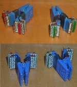
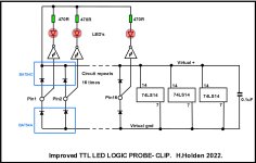
One interesting thing about this LED probe, the intensity of the LED gives a clue as to the likely duty cycle of pulses on the pins. In this case HP used very small sized red LED's. These sorts of clips are easy to make too with a logic test clip and adding LED's, I have posted the design of one before. It is not just if the LED is lit, or not, there is more information there in the case that they are lit up.

Imagine for example; a camera was set up and the clip was moved to all of the 16 and 14 pin TTL IC's on the PET board and a photo was taken and assembled into a large photo. The photo would show a gigantic pattern indicating the conditions of all the IC's each with their own unique LED light pattern. In a way, it would be somewhat similar to the IR photo and the image could be used as a type of reference in fault finding PETs.

Of course the LED logic probe is no substitute for a scope. But it still can provide useful pattern recognition information, provided there is a known normal reference pattern for each IC on the board.
 

Attachments

  • pattern.jpg
    pattern.jpg
    193.7 KB · Views: 16
I'd happily help out if you can point me at your post (and I'm technically proficient enough to build it).

That HP probe looks really good. Also looks difficult to find.....

Colin.
 
I'd happily help out if you can point me at your post (and I'm technically proficient enough to build it).

That HP probe looks really good. Also looks difficult to find.....

Colin.
Yes its is on that thread Daver2 referenced.

I made a couple of these in the past, I just used proto board, it would be much better if it was rectangles of real pcb's.

The red & black crossing wires are the virtual gnd and the virtual supply created by the 1N4148 diodes.

Also, one thing I did not think of at the time, it would have been better to use clear LED's, or surface mount ones with a small surface area of the diode junction, rather than the ones with diffused colored plastic, because if you take a flash photo of the diffused one, the plastic illuminates the similar color to the diode junction and the contrast of the photo is not as good. There are lots of good small surface mount diodes out there now, so I think the design could be improved. I would do a better job on these if I was re-making them now.

As I mentioned, I had no idea what was inside the professional units. I would open up my new HP probe , but wouldn't you know it, they have made that very difficult without damaging it. The one I got recently was NOS and in perfect condition, but it was costly at $75. I got it because I had a nostalgia attack and remembered using one back in the 1970's. HP also make a version that does higher voltage ranges for cmos.

I had to dream up the idea of the virtual ground and the virtual supply created by the diodes to make mine work, because it has to work regardless of which pins are supply and ground or which way around it is clipped on the IC. But there might be an entirely different way to do it, that I'm unaware of. If anybody has the schematic of a commercial one, I would be very interested to see it, if they did it the same way, or not.
 

Attachments

  • probes4.jpg
    probes4.jpg
    196.1 KB · Views: 9
Last edited:
Hugo,

If I remember correctly, there was a design for one many, many years ago in the Practical Electronics publication in the UK. I believe that used an identical technique of diodes for the virtual supply rails.

Dave
 
Yes - I'm afraid that's beyond my abilities as I feared.

I'll keep my eye out for one of the HP probes, but they look a bit spenny.

Colin.
 
Practical Electronics January 1976 page 52. See: https://worldradiohistory.com/Practical_Electronics.htm.

They condensed Hugo's circuitry down to one resistor, one diode and one LED per pin.

Dave
Hi Dave,

Thanks for posting that. I knew one day I would find that circuit. How did you find it I wonder, did you remember it from back then ?

Each pin pair of their design has 2 LED's, 2 diodes and 2 resistors.

Each pin pair on mine has 2 LED's 4 diodes and 4 resistors , due to the creation of the virtual + rail in mine.

The main difference being that they just used a virtual or common ground like mine and didn't bother with the virtual plus rail. So this saved 2 diodes and two resistors per pin pair.

So what is the advantage of the virtual + rail ?

One reason that I thought it was good to have the virtual plus rail, apart from the circuit symmetry, was so I could craft the circuit so that the probe's pin connections (that were not either the Vcc or gnd ones) in the open circuit condition sat at logic high for TLL or about 3.5 V, and lit the LED in an output pin open circuit condition. The reason is that this is the way a floating TTL input connected there would interpret it. And the input current of a TTL pin on its own is not enough to light the LED significantly and the probe itself could possibly pull the line logic low, on an open circuit output pin. The presence of the probe itself therefore altering the conditions of the test. So that was the "logic" of the virtual plus rail, though it uses more parts.

The two designs are a little different on that point.

I like the design of their clip too though, with the side rather than top viewing LED's, very cool retro look.
 
.. ...though further to the above remarks, the fwd drop of the LED would likely prevent the open circuit pin likely being pulled below logic low, but the LED would still not be well lit by the small gate input source current, showing a low, when really it would be acting as a high for any inputs connected to the open circuit output pin. So, despite the extra parts, I think the + rail is worth it.

Now I know what was in that Practical Electronics probe, I can perform a test on the HP probe and see if it conforms to that design, will be interesting.
 
Hugo,

I remembered it was in Practical Electronics (I subscribed to Practical Electronics, Everyday Electronics and Electronics Today International back in the day) and roughly the decade. A search in the online archive of Practical Electronics nailed the issue.

Yes, your design is 'orthogonal' - hence the additional components.

Dave
Dave,

I have just come up with an improved LED logic probe. See attached.

In essence you want the probe to tell you if the IC pin is logic high or low according to TTL specs, regardless of whether there are pulses and average LED brightness modulation from their duty cycle.

The thought occurred to me that the ideal "diagnostic sensor" to determine the logic state of the TTL's IC pin, is not an LED directly, but nothing other than a TTL gate input, which will determine the logic state according to TTL standards and hard switch the LED if a Schmitt trigger IC is used.

So I have re-designed it using my virtual + and virtual ground method to power some hex inverter IC's. These would be SOIC package types to keep it compact and a shift to surface mount Schottky diodes to keep the voltage drops low as possible. Interestingly a lot of the resistors of the original design are eliminated. I have not built this yet but I think it will work. I don't think the fact that the IC's input voltage will go a little higher and lower than the IC's supply rails will hurt. If there was a problem I could try an HCT family IC. or possibly put back to back diodes in series with the IC input, but I'd prefer not to add any parts.
 

Attachments

  • NEWPRB.jpg
    NEWPRB.jpg
    162.1 KB · Views: 5
Funnily enough, I was thinking of a similar thing...

Although I was thinking a bit more costly and using operational amplifiers and a stabilised potential divider chain to determine HIGH, LOW and INVALID logic states. Possibly with a RED/GREEN LED.

Dave
 
Funnily enough, I was thinking of a similar thing...

Although I was thinking a bit more costly and using operational amplifiers and a stabilised potential divider chain to determine HIGH, LOW and INVALID logic states. Possibly with a RED/GREEN LED.

Dave
That is a good idea !

It could have dual LED, Red high Green low and say a mix like yellow indeterminate/invalid logic state.

It is that indeterminate state that could find some defective gates.
 
......... on the topic of using OP amps as slicers with resistive divider chain references, I recently did this in an unbeatable Tic Tac Toe computer I designed. This is so the player pieces (which contain weak magnets) can be identified as X or O or not present on the player board. This results in the generation of 18 data bits to address a ROM. The OP amp effectively examines the output of linear Ratiometric Hall sensors embedded in the player board:


(this game also deployed a Parity IC which was a novel use for one in the game sequencer circuit, to allow for who starts the game first, the Human or the machine)

One interesting thing, the LM324 OP amp is suited to the task of interfacing with TTL, because of the design of its output stage, its voltage swing practically exactly matches TTL highs and lows when the OP amp is powered by 5V.
 

Attachments

  • SLICER.jpg
    SLICER.jpg
    75.9 KB · Views: 6
Back
Top