• Please review our updated Terms and Rules here

PDP-11/34 restoration

thunter0512

Veteran Member
Joined
Sep 27, 2020
Messages
859
Location
Perth in Western Australia
I am restoring a PDP-11/34 in what I think is a BA11-K box and found the 11/34 related manuals & drawings on Bitsavers.

While restoring my LAB-8/e and PDP-8/e I found the 8/e maintenance manuals with detailed theory of operation very useful.

I could not find the same level of detail for the 11/34. Do such documents exist for the 11/34.

Specifically other than schematics I found nothing about the power supply modules H744 (5V 25A), H745 (-15V 10A) and H754 (20V 8A, -5V 1A).

Questions:
  1. Are there documents which describe the "theory of operation" of the H744, H745 and H744 power supply modules.
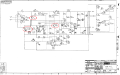
  2. Are there better schematics of these power supply modules than found in "MP00082_1134_Vol2_Sep76.pdf" from Bitsavers with the title "11/34 Vol 2 Field Maintenance Print Set".
My difficulty with these schematics is that they can be ambiguous because interconnects are not shown as dots.

My plan is to get all power supply rails stable and then start debugging the M7265/M7266 CPU boards and KY11-LB programmer's console.
I expect a steep learning curve as I have never even seen any PDP-11 before.
 
Under http://bitsavers.informatik.uni-stuttgart.de/pdf/dec/pdp11/1134/ If you haven not already reviewed it see the CPU maintenance manual for theory. There is no crystal in the 11/34 like a microprocessor. Timing of CPU clock cycles depend on the state of the of machine and can be variable. See page 4-50.

As far as power supply theory of operation, I'm not aware of any documentation. That said, they look like linear regulators with over-voltage protection and logic signal of readiness. The general feeling is that the transistors are the fuses in some DEC designs. There may better and/or different resolution scans of the same H744/H745 schematics in documents like PDP-1140_System_Engr_Drawings_Rev_P_Jun74.pdf

Jerry
 
Last edited:
As far as power supply theory of operation, I'm not aware of any documentation. That said, they look like linear regulators with over-voltage protection and logic signal of readiness.
Actually the supplies are all switching regulators not linear ones despite the presence of an LM723 in each circuit.
Note the inductor and diode after the pass transistors.
 
Actually the supplies are all switching regulators not linear ones despite the presence of an LM723 in each circuit.
Note the inductor and diode after the pass transistors.
Yup, I blew this. The 11/34 (and 11/40?) had switching.
 
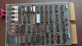
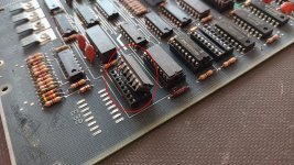
The M9312 Bootstrap Terminator board in my 11/34 has been mis-treated.

One of the PROMS (E35) has been partially ripped out. I wonder if this was part of a debug/repair attempt? All the output pins are in the air which may mean this was intentional, not an accidental damage.

Also I am confused about E33 which is a tri-state N82S131N as opposed to the other PROMS which are open-collector MI-7621. Strangely the N82S131N has the valid DEC 765A9 marking. I would not expect tri-state and open-collector PROMs on the same data bus.

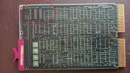
Finally the messily soldered 0R resistors (W1 - W6?) near the edge connectors make no sense to me compared the M9312 Field Maintenance Print Set (Rev. A). I wonder where the documented W7 - W12 are? Likely the manual revision does not match my board.

I would appreciate any help and or suggestions. I am new to the PDP-11/34 world.

Here are the relevant photos:

IMG_20230906_103634371.jpg

IMG_20230906_103646958.jpg

IMG_20230906_103731582.jpg
 
I must say that you have an “interesting” example of an M9312 and that I would not expect it to work well in a PDP-11/34 configured as is. Referencing http://www.bitsavers.org/pdf/dec/unibus/M9312_TechRef.pdf as well as my own M9312 from a functional 11/34A, I can see three immediate concerns:
  1. Jumpers W1, W2, W3, W4 and W5 should all be removed (see page 1-6 in the manual).
  2. Although difficult to read, it appears that you have a “757A9” ROM (partially) installed in socket E35. I find that curious as another “757A9” seems to be installed immediately below it in socket E34. Both of those are intended to boot from a TU16 tape drive but why two? Also, the ROM in socket E33 is marked “755A9” which should boot from an RP or RM disk. I wonder if this M9312 was native to your machine - do you really have a TU16 or any RP or RM disks?
  3. You are also missing a cap next to E1 (lower right corner).
The good news is that you apparently have a console emulator and diagnostic ROM installed in socket E20, so if you rectify the jumper situation you may be able to get an ASCII console working. I'll be interested to hear how your restoration develops.
 
Thanks for the info.
I too thought that W1 - W6 should not be fitted, yet they are fitted.
The partially fitted E35 is a "752A9" ROM not a "757A9". I have no idea about the state of my machine. It may well be a collection of random boards.
There is only a bit of wire sticking out next to E1. I wonder what this cap is meant to be. It looks as if it has either snapped off or was cut out.

I am working on reviving a dead H745 supply (-15V 10A). I am suspecting the LM723.
 
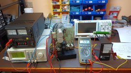
Today I fixed the faulty H745 supply (-15V 10A). As suspected the LM723 voltage regulator was dead. Replacing it was made harder than necessary by DEC who bent all 14 pins hard down to the PCB surface defeating my vacuum desoldering station. If the pins stick up a little I can heat, suck and then gently bend the pins straight. When the pins are flat on the surface the desoldering tip can't grab the pins. I had to cut all pins and desolder them one by one.

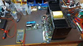
With a new LM723 fitted and the PCB cleaned up it works perfectly. I am load testing at the moment with a 15 Ohm 120W resistor and it has worked perfectly for the past hour or so. Here is a photo:

IMG_20230907_182703332.jpg

The large 31000 uF filter cap on the 30V input rail is not yet fitted because the 30V from the bench supply is stable. It is much easier to work on this supply with the large cap removed.
 
I have resolved several power supply issues, but the final issue is the initially working H754 (+20V 8A -5V 1A) which after I assembled it into the BA11-K box now no longer works.

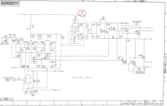
The problem is that something appears to short the 15V voltage for the LM723 created by R3 (1.5k 5W), D3 (Zener 15V), C11 (2.2uF) and Q5.

I have already replaced the burned and open-circuit R3 and now I measure 0.96V across C11 not the expected 15V.

Could someone less tired and confused then me please look at the schematic below and suggest possible culprits. I have already tested D3 and C11 in-circuit and they appear to be fine. I am pretty sure about Q5 too.

h754 15V short.png

I am testing in-circuit because non-destructive component removal is almost impossible in many cases because of the darn pin bending.

Thanks
Tom
 
D9 appears to be a crowbar that will pull the 15V node down if the +20V or -5V outputs are too large. And being an SCR, once it's conducting it stays conducting. What should be +15V travels through D13, D9 and D8 to ground, so I'd expect a bit more than 0.96V, but still it's something I'd look at.
 
Thank you very much Steve. Your analysis of the problem was spot on.

Here is what happened:

I initially tested the H754 on the bench with a smaller 24VAC transformer (as opposed to the 28VAC of the BA-11K transformer) powering the unit. I adjusted the +20V and -5V rails and then load tested the unit with some resistors. I did this with all four supplies and also replaced the faulty LM723 in one of the H745 (-15V 10A).

Subsequently I reassembled everything back into the BA-11K and after testing all supply rails the previously working H754 appeared to be unexpectedly dead. After removing the H754 and putting it back onto my 24VAC supply on my bench I messed with the +20V and -5V adjustment pots without any change in output voltage. Eventually I noticed that there was no +15V on V+ of the LMC723 and found that R3 was somewhat browned (and corroded) and open circuit.

Once I fitted a new R3 the circuit should have worked, but because of my previous messing with the +20V and -5V adjustment pots the crowbar circuit now pulled the +15V down to 0.96V.

My earlier +20V and -5V rail adjustments must have been close to the crowbar limits and by now operating with a higher AC input (now 28VAC versus 24VAC) resistor R3 failed by a combination of old age and the circuit being for a while in the "crowbared" mode while I tested all the other rails.

All I needed to do was to turn both +20V and -5V adjustment pots fully CCW to get the +15V supply for the LM723 back.

Thanks again!
 
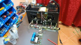
The BA11-K is now mostly reassembled and all voltage rails are nicely adjusted and stable. Here are 2 photos (click on the photos to see full size):

IMG_20230909_210325299.jpg

IMG_20230909_211317699.jpg


The 5411086-0-1 (+15V reg and AC low & DC low sensing) is still not mounted in the power input box because of some heat concerns.
 
Speaking of heat concerns ...

While checking out the supply rails I noticed a bit of heat coming from the 5411086-0-1 (+15V reg and AC low & DC low sensing). When looking closer, the heat comes from R8 a 470 Ohm 2W resistor. The resistor R8 is dropping 27V of the 37V and the resulting 10V is is then fed into the chopper circuit (Q3, Q5 and T1) which on the secondary side of t1 generates -12VDC used as the negative bias for JFETs Q14, Q15, Q17 and Q18.

The current through R8 is 57mA and the voltage drop of 27V means about 1.5W. The resistor is rated 2W so that should be OK, but the solder side of the PCB under R8 nevertheless gets up to about 70 degrees Celsius. After power off I measured about 680 Ohm which slowly dropped towards 470 Ohm as the resistor cooled. I don't think this is good so am considering replacing the 2W carbon resistor with a 5W wire wound resistor.

Any thoughts?

Here is the circuit (please click on it to see it full size):

5411086-0-1 hot resistor.png
 
You could take a look at the current and voltage on R8 with an oscilloscope. I think that you will find that the current through the resistor looks more like an AC signal than a DC signal, so measuring the voltage and current with a DVM might give your the wrong answers. All of the switching current for T1 is going through R8, so DEC made it a 2W part to handle the power. It is probably OK for another 30 years.
 
There is a mighty big 8400 uF cap after the bridge rectifier. The 57mA was not measured but calculated based on the voltage drop across the resistor. The 5W resistor is physically larger with a ceramic body, so I was thinking it would handle the sustained heat better than the carbon version. Maybe an alternative would be to replace the 460 Ohm 2W resistor with a 560 Ohm 2W (or even larger). Or maybe as you say just leave it in peace. :)
 
Back
Top